
Introduction to KiCad on Ubuntu
Learn how to install the new and improved KiCad on Ubuntu 15.04 and then build a simple microcontroller board to blink an RGB LED.
Recommended Level
Intermediate
Introduction
Looking to build a circuit to automate your home, a la Nest? What about a custom camera add-on for your quadcopter? How about a sneakier and more compact booby trap alarm system? There might be commercial products out there that accomplish what you want, but the most flexible and often cheapest way is to jump into the world of electronic circuit design and do it yourself with the help of free software tools.
There are many electronic design automation (EDA) tools on the market for creating printed circuit boards. Some, like Altium Designer and Cadence OrCAD, are incredibly powerful but are geared toward businesses and can cost upwards of $7,000 USD per license. There are also several popular hobbyist PCB design tools that are free (as in beer) such as Cadsoft Eagle (Cross Platform), Altium CircuitMaker (Windows Only), and RS Components DesignSpark (Windows Only). They all have their pros and cons but my complaint with them is that they are all proprietary, closed-source programs. One answer to this is KiCad.
KiCad is a very powerful, fully open-source electronics design program that is getting better every day. In 2013, as part of their Open Hardware Initiative, CERN began contributing both expert development skills and funding for some really great features. It's also been used for very complicated professional products such as the HackRF One, Ubertooth One, Smoothieboard CNC controller, and many more. In the spirit of open-source, this tutorial will focus on getting a working installation of KiCad on Ubuntu 15.04 and creating a simple microcontroller board for use in future electronics projects.
What You Need
- A computer running Linux with an internet connection. This tutorial is catered specifically to Ubuntu 15.04
Installation
The stable version of KiCad that's available in most package managers is very old and doesn't contain the improvements from CERN since the source code repository is under such active development. Unfortunately, that means this is going to be slightly more complicated than simply typing sudo apt-get install… KiCad at this point needs to be built from its source code. Even though this sounds complicated, there's no need to worry since there is a very conveneient helper script provided by KiCad to make this process easier. From the Electronics Design on Linux by Trevor Gamblin we're going to have to use some basic Bash commands to navigate the terminal.
If you happen to be on a different platform than Linux, KiCad provides some instructions on getting you up and running with Windows and Mac OS X.
The first step is to download the helper script here.

Download it to your home directory and open a terminal. If you aren't there already, change directory to your home folder:
cd ~ # The tilde is your home directory in Linux shorthand
Now, open the file in a text editor. Since we're getting famililar with the command line, we'll use nano for this example:
nano kicad-install.sh
Read through the comments at the top of the file (they start with #) and then scroll down to the first line of actual code which reads:
WORKING_TREES=~/kicad_sources
This is personal preference, but I don't like to have installation files right in my home folder (it clutters it up), so I tuck them away in a hidden folder called .opt. On my script, that line looks like:
WORKING_TREES=~/.opt/kicad/kicad-sources
Now since we want to work with the CERN improvements, make sure the line that sets the REVISION variable is set to $TESTING
# Set this to STABLE or TESTING or other known revision number:REVISION=$TESTING
I also uncommented (deleted the # in front of) the line below that which allows for third party python scripting to help automate and enhance board design down the road.
# More advanced python scripting: gives access to wizards like footprint wizards and creates a python module# to edit board files (.kicad_pcb files) outside kicad, by python scriptsOPTS="$OPTS -DKICAD_SCRIPTING=ON -DKICAD_SCRIPTING_MODULES=ON"
It's still always a good idea to read though the rest of the script and get a gist of what it's trying to do but at this point, we're done editing and can save and close the script with +X, Y, .
The next step is to enable execution in bash so we can run it from the terminal:
chmod +x kicad-install.sh
Now run the script by typing:
./kicad-install.sh --install-or-update
After you type your password, this process should be more or less on autopilot but it will take a long time to install (likely over a half hour) and could make your computer seem sluggish in the meantime. You'll see a lot of what looks like gibberish in the terminal but that's just the cmake program letting you know what it's doing. Grab a coffee and come back in a bit.

It's gonna be a while...
Eeschema Schematic Editor
Now that we have everything installed and ready to roll, we're going to build a basic circuit in the schematic editor and then lay everything out on a board. This circuit is going to use an Atmel ATtiny85 microcontroller to blink an RBG LED all while running off of an external battery pack. This tutorial will only cover the fundamentals of Eeschema and Pcbnew. Next time, we'll go into greater detail about creating custom parts and exploring some of the intricacies of the KiCad EDA suite.
Begin by typing kicad into your terminal. You should be greeted by a very vanilla-looking user interface with some panels and buttons. Create a new project by navigating to File > New Project > New Project or by typing +N. I called my project aac-demo.pro.

Now, open the schematic editor, Eeschema, by clicking the block that looks like this: ![]()
You'll be asked to create a new schematic file so just clik OK and then you'll be greeted with an empty schematic page. Begin adding parts by either using Place > Component in the menu at the top or by just pressing the “A” key.

Component selection dialogue
Here you can select your microncontroller and everything else you'll need in the circuit. Using the filter, type “ATTINY-85P” which is the through-hole version of the ATtiny85 (8k Flash, 512B SRAM, and 512B EEPROM). Click OK and place it somewhere on the schematic. Press “A” again and add the following parts to your project. You can also duplicate parts by hovering over them and pressing the "C" key:
- 4x R (Resistor)
- 3x C (Capacitor)
- 1x LM7805CT (Voltage regulator)
- 1x SW_PUSH (Push button)
- 1x LED_RCBG (Common annode RGB LED)
- 1x CONN_01X02 (Battery connector)
- 1x CONN_02X03 (Programming header)
It is worth noting that in most EDA software packages, you can technically accomplish everything through the menu or with buttons, but one of the biggest aids to productivity is using the hotkeys built into the software. From this point, I will instruct you with hotkeys instead of menu buttons if possible since they are faster and less complicated. If you need to be reminded of the hotkeys at any time, pressing “?” in Eeschema or Pcbnew at any time will pull up a helpful hotkey window like this:

With all that all of your parts have been added, yous schematic should look something like this:

Next, we'll put together the voltage regulator circuit. This takes the external battery pack and regulates it to a cool 5V so that we don't blow up our chip. Move the LM7805 regulator to an unihabited part of your page by hovering over it and pressing “M” (for move). Also move the CONN_01X02 and two capacitors. Arrange the parts neatly and start connecting everything with wires by pressing the “W” key. You can also rotate parts 90 degrees by using “R”. So far you should have something like this:

As a side note, those green circles correspond to electrical junctions and can be added manually with the “J” key.
Next, we need to specify the capacitor values. The LM7805 datasheet recommends 0.33μF on the input pin and 0.1μF on the output. Edit the capacitor parameters by pressing “E” and changing the Field Value of the Value parameter to the corresponding capacitance. Don't worry about the 'C?' in Reference for now. There is a tool we'll use later to automatically assign a numeric reference to each part.

The last stage of the power supply block is to add power flags. These “net names” act like sort of like global variables in programming and correspond to the voltages our circuit is using. Press “P” to open up a dialogue similar to the part selection one and add the following power rails to the circuit:
- +BATT
- +5V
- GND
Connect them to the circuit at the appropriate points and the power supply section is complete.

Next, using what you've learned so far, connect up the rest of the circuit like so (don't forget about updating the resistor and capacitor component values as well):

The last thing that needs to be connected in the schematic is the 2x3 programming header and the switch. In order to keep things modular and clean, I like to use labels. Any wires with the same label are connected schematically without the visual clutter of wires running across the page. Press the “L” key to make a label and update the circuit accordingly:

To complete the schematic, we need to assign unique references to each of the parts through a process called annotation. Press the  button on the toolbar or go to Tools > Annotate Schematic. Keep the default settings and press OK. The schematic is now complete.
Match Parts to Footprints and Generate a Netlist
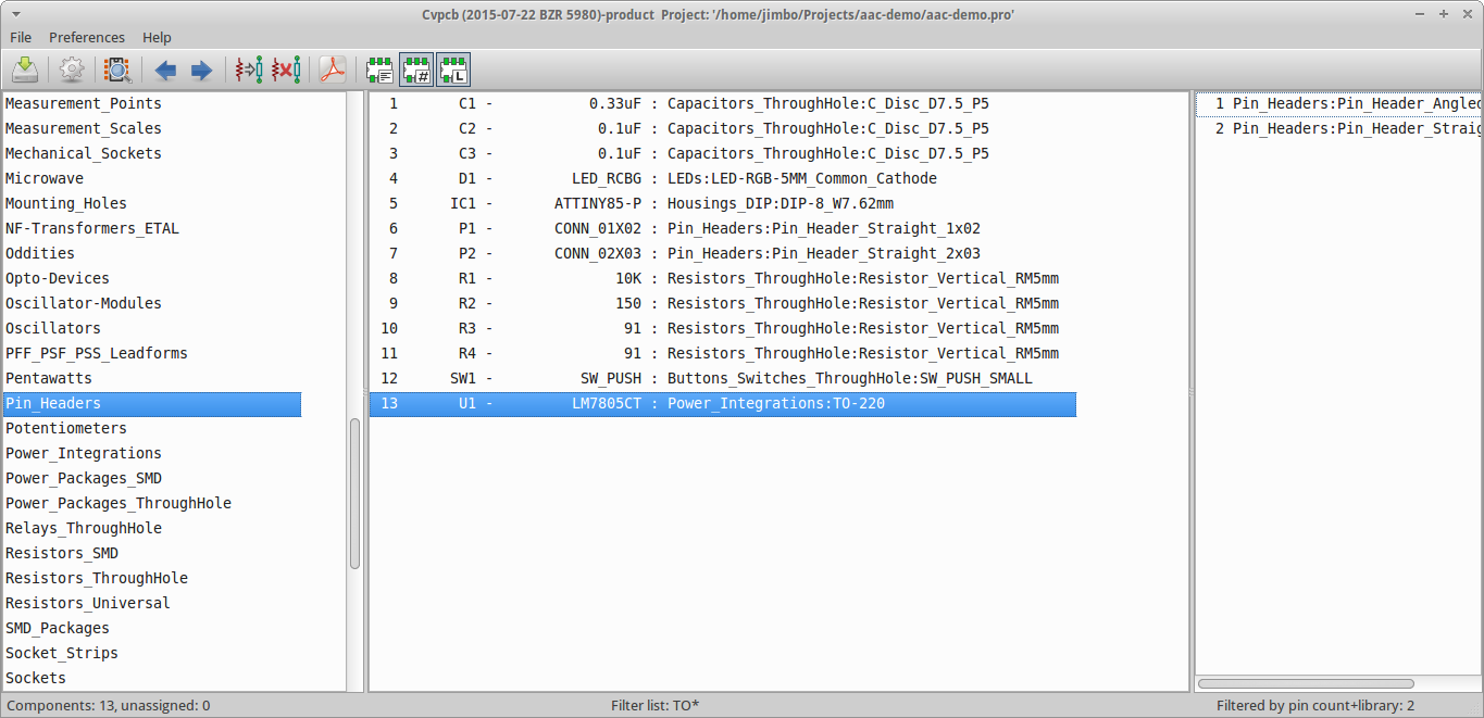
The next step is to associate the schematic parts with the footprints that will appear on the printed circuit board and create a netlist file that can be imported by the Pcbnew layout program. This process is some somewhat clunky in KiCad and still needs some polishing before the final release. Press the  button on the toolbar or select Tools > Assign Component Footprint to open up the CvPcb program. Mine tossed an error when I opened it complaining about legacy footprints. Just press OK.

The program presents you with three columns. From left to right, they are the available footprint libraries, the components in your schematic, and the individual footprints in the selected library that match the filters. Filters can be turned on and off by pressing the  buttons on the top. To associate a footprint for the capacitors, for example, I select the "Filter Footprint List by Library" filter button, select the Capacitors_ThroughHole library on the left column, select C1 in the middle column, and double click the C_Disc_D7.75_P5 footprint.

Using this method, associate the following footprints with their respective parts:
| Library | Part | Footprint |
| Capacitors_ThroughHole | Capacitors | C_Disc_D7.75_P5 |
| LEDs | LED_RCBG | LED-RGB-5MM_Common_Cathode |
| Housings_DIP | ATTINY85-P | DIP-8_W7.62 |
| Pin_Headers | CONN_01X02 | Pin_Header_Straight_1x02 |
| Pin_Headers | CONN_02X03 | Pin_Header_Straight_2x03 |
| Resistors_ThroughHole | Resistors | Resistor_Vertical_RM5mm |
| Buttons_Switches_ThroughHole | SW_PUSH | SW_PUSH_SMALL |
| Power_Integrations | LM7805CT | TO-220 |
The middle column should look like this when you are finished:
If you are having trouble finding the right parts, try playing with the filters to see if the footprint will show up in the right-hand column. These are all default libraries so everything should be there in a fresh install. If you want to see what the footprint looks like, press the  button.
Make sure to save these edits and then exit the program back to Eeschema. Back in the schematic editor, press the  button to generate a netlist file. Keep the default settings and select OK. We're now ready to begin laying out our board in Pcbnew.
Pcbnew Layout Editor
Now it's time to finally lay everything out on the PCB. Select the  button either in Eeschema or on the KiCad welcome window to open Pcbnew. After thcreating the file, you will then be presented with another blank sheet similar to that in Eeschema. Locate the button at the toolbar on top to import the footprints we assigned in CvPcb into Pcbnew. Keep the default settings and select Read Current Netlist. The netlist reader is also what you would use to update the PCB with new changes in the schematic.

Netlist reader window
With any luck, you should have a garbled mess of footprints all stacked on top of each other. KiCad includes a handy tool for dealing with this by allowing you to spread everything out on the PCB. Find the  button on the toolbar at the top to put Pcbnew into "Footprint Mode" -- this enables a special context menu for dealing with footprints. Right click the mess and select Global Spread and Place > Spread out All Footprints like so:

Ahh, much better. At this point, the art of PCB arrangement starts taking over. Using the "M" key to move parts and "R" to rotate, begin placing the parts in a way to minimize traces crossing each other. Generally this means keeping the white ratsnest lines from intersecting as much as possible but like I said, this is more art than science, so just play around with it. KiCad also has several view modes. I prefer the OpenGL View which you can enable with F11. My finished arrangement of parts looks like this:

Now we can begin routing. Hover over a pad and press the "X" key. This will begin drawing a line on the board which represents a copper trace. The Page Up and Page Down keys allow you to switch between the top and bottom copper layers and pressing "V" will create a via to jump from one layer to the other. Since this board used all through-hole parts, I was able to route it without any vias. It's also important to define where the end of your board is so click the Edge.Cuts layer from the right panel and select the Graphic Line or Polygon Tool to create some sort of closed shape around your board. It doesn't necessarily have to be a square:

Routed board with a pentagonal outline
Add flair and annotations by selecting the Text button on the right panel. To add them to the decorative top layer called the silkscreen, select F.SilkS as the layer of choice.

Finally, the "O" key will allow you to add arbitrary footprints which is useful for adding things like the Open Source Hardware Logo.
![]()
Once you have everything where you want it and consider the board finished, check it out in 3D by pressing +3

Conclusion
This is only a basic overview of what KiCad is capable of. It supports differential pairs for high frequency circuits, custom part creation, generation of Gerber files to be sent off for manufacturing, hierarchical schematics, and MUCH more. Other tutorials in the future will unpack some of the intricacies of KiCad, but for now you are well on your way to making PCBs. If you would like to see some more information and tutorials in the meantime, Chris Gammell (of Amp Hour fame) over at Contextual Electronics has a YouTube channel filled with awesome tutorials and information on KiCad and electronics in general. I definitely recommend checking it out. Until next time... happy hacking!


Thanks for the well-written KiCad tutorial.
By the way, as of ***buntu 16.04 (Ubuntu, Xubuntu, Lubuntu, etc.), kicad and its relatives are packages of the “Electronics (universe)” repository.