Conversion of D Flip-Flops
This article presents the conversions of D-type flip-flops into SR-, JK- and T-types. It also explains how to verify the conversion process.
This article presents the conversions of D-type flip-flops into SR-, JK- and T-types. It also explains how to verify the conversion process.
Previous Articles in This Series
- Conversion of Flip-Flops — Part I
- Conversion of Flip-Flops — Part II
- Conversion of Flip-Flops — Part III — JK Flip-Flops
Introduction
Here, we will briefly present the methodology to convert the given D flip-flop into (i) an SR flip-flop, (ii) a JK flip-flop and (iii) a T flip-flop; this process is discussed in detail in Part I of the series.
Next, we will verify the resultant systems using the technique described in detail in Part II of the series.
Conversion of a D to SR Flip-Flop
The process of converting the given D flip-flop into an SR-type is initiated by obtaining a table which represents both the information present in the truth table of the SR flip-flop as well as the information conveyed by the excitation table of the D flip-flop. Such a table is referred to as the D-to-SR conversion table and is shown in Figure 1.
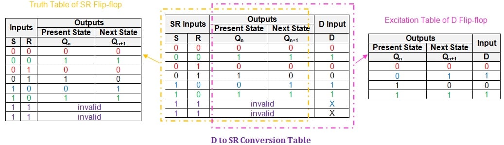
Figure 1: D-to-SR conversion table. Click to enlarge.
Here we note that the last two rows of the conversion table have X (Don't Cares) in the "D Input" column. This is because with an SR flip-flop the input combination of S = R = 1 is invalid (because the output will be unpredictable).
Our next step will be to obtain the logical expression for the input of the given D flip-flop in terms of the inputs of the desired flip-flop, S and R, and the present-state, Qn. However, while doing so, we need to simplify the Boolean expression as much as possible using a suitable simplification technique, such as the K-map. The Karnaugh method is covered in detail here.
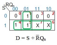
Figure 2: K-map Simplification for D input
From Figure 2, the simplified logical expression for the D input is found to be S + R̅Qn. This means that, in order to make the given D flip-flop behave like the desired SR flip-flop, we need to AND Qn with the negation of the user-defined input R and then OR the result with the user-defined input S.
Thus the additional combinational circuit required would be one NOT gate, one AND gate, and one OR gate. The resultant system, designed using these components, is shown in Figure 3.
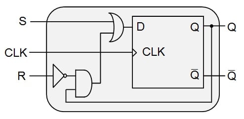
Figure 3: D flip-flop behaving as an SR flip-flop
Upon completion of the conversion process, we need to move on to the verification process. Here, we need to write the truth table for the designed system and compare its entries with those in the truth table of the SR (desired) flip-flop.
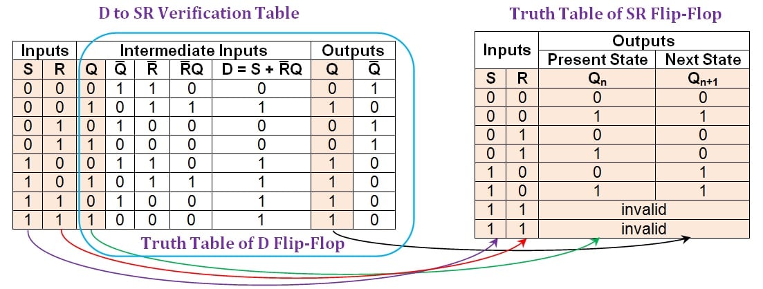
Figure 4: Comparison between the D-to-SR verification table and the truth table of an SR flip-flop. Click to enlarge.
The figure shows that all the entries in the first, second, third, and eighth columns (shaded in beige) of the D-to-SR verification table are consistent with those present in the truth table of the SR flip-flop. The last two rows appear to differ, but they can be considered equivalent because an SR flip-flop's outputs can be either high or low as a result of the invalid input combination. Actually, we have designed a system that is better than an SR flip-flop because it has predictable output behavior when both inputs are high.
The verification table indicates that the conversion process was a success: The given D flip-flop was made functionally equivalent to the desired SR flip-flop.
Conversion of D to JK Flip-Flop
The given D flip-flop can be converted into a JK flip-flop by using a D-to-JK conversion table as shown in Figure 5. This table collectively represents the data of both the truth table of the JK flip-flop and the excitation table of the D flip-flop.

Figure 5: D-to-JK conversion table. Click to enlarge.
Following this, we need to simplify the expressions for the D-input in terms of J, K, and Qn. We will again employ the K-map technique.
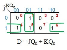
Figure 6: K-map simplification for D input in terms of J, K, and Qn
Figure 6 shows that, in order to convert the D flip-flop into a JK flip-flop, its D input needs to be driven by the output of a two-input OR gate which has its inputs as
- J ANDed with the negation of the present-state Qn (i.e., Q̅n)
- Negation of K (K̅) ANDed with the present-state Qn
This indicates that we would require
- One NOT gate—to negate K
- Two AND gates—one to obtain JQ̅n and the other to get K̅Qn
- One OR gate—to obtain the D input given by JQ̅n + K̅Qn
Thus, the resultant system would be as shown in Figure 7.
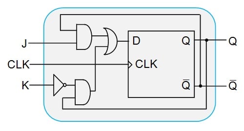
Figure 7: The D flip-flop designed to behave as a JK flip-flop
Lastly, let us verify whether our designed system behaves as we expect it to using a D-to-JK verification table, shown in Figure 8.
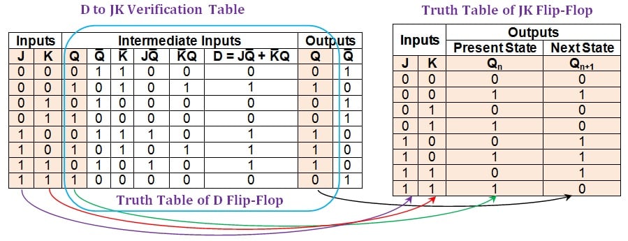
Figure 8: Comparison between the D-to-JK verification table and the truth table of a JK flip-flop. Click to enlarge.
Figure 8 shows that the first, second, third, and ninth columns of the D-to-JK verification table (shaded in beige) have entries which are identical to those in the columns of the JK flip-flop's truth table. This indicates that the given D flip-flop behaves exactly as a JK flip-flop for every combination of inputs and the present-state.
Thus, we can conclude that the conversion process was successful.
Conversion of D to T Flip-Flop
In order to convert the given D flip-flop into a T-type, we need to obtain the corresponding conversion table, as shown in Figure 9. Here, the information in the excitation table of the D flip-flop is inserted as a part of the T flip-flop's truth table.
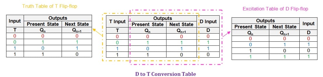
Figure 9: D-to-T conversion table. Click to enlarge.
Having obtained the conversion table, the next step is to express the input, D, in terms of T and Qn.
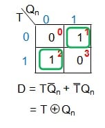
Figure 10: K-map simplification for D in terms of T and Qn
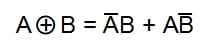
From Figure 10, we see that in order to convert the given D flip-flop into a T-type, we need to drive its input pin (D) by the output of an XOR gate whose inputs are T and Qn. This would lead to the new digital system which is shown in Figure 11(a).
If we must confine ourselves to only NOT, OR, and AND gates, we will need to follow these steps:
- Use an AND gate to AND the user-defined input, T, and the negation of the flip-flop's present-state Qn.
- Use another AND gate to AND the present-state of the flip-flop with the negation of T (obtained as an output of a NOT gate).
- OR together the outputs of the two AND gates using a two-input OR gate.
This leads to the digital system shown in Figure 11(b).
.jpg)
Figure 11: D flip-flop designed to behave as a T flip-flop using (a) an XOR gate and (b) only NOT, OR, and AND gates. Click to enlarge.
The next and final step is to verify the conversion process using the D-to-T verification table, shown in Figure 12.
.jpg)
Figure 12: Comparison between the D-to-T verification table and the truth table of a T flip-flop. Click to enlarge.
From the figure, it can be seen that the first, second, and penultimate columns (shaded in beige) of the D-to-T verification table are identical to the columns in the truth table of the T flip-flop. This indicates a successful conversion process, i.e., the given D flip-flop behaves exactly as a T flip-flop.
Although we have verified the system designed in Figure 11(a), the conclusion is valid also for the design shown in Figure 11(b) because
Summary
This article presents the methodology used to convert a given D flip-flop into SR-, JK-, and T-type flip-flops. It also discusses the verification process for each of these conversions.
The next part of the series (Part V) will cover the conversion of a T flip-flop into other types.