
How to Buffer an Op-Amp Output for Higher Current, Part 1
Op-amps become even more versatile if you can use them in high-current applications. In this article, we will look at a basic current-buffering circuit.
You can greatly increase op-amp output current with little more than a single bipolar junction transistor.
Supporting Information
Do We Need a Current-Buffering Circuit?
Op-amps are versatile, to be sure, but their range of applications is restricted by their output-current limitations. A typical op-amp can be expected to continuously sink or source not more than 30 or 40 mA, though some parts can handle closer to 100 mA, and others will struggle to give you 10 mA. There is a special category of high-output-current amplifiers, with current capability approaching or even exceeding 1000 mA. If a high-output-current part is compatible with your application, by all means use it. But there are a few reasons why you might prefer to buffer the output of a more general-purpose amplifier. First, some high-output-current amplifiers are sophisticated parts intended for specialized applications, and consequently, they are less versatile and more expensive—for example, the LT1210, a Linear Tech part that can drive 1100 mA, will set you back $12 if you’re buying in low quantities. Furthermore, some high-output-current parts (including the LT1210) are current-feedback amplifiers, and you can’t simply drop a current-feedback device into a circuit designed for the voltage-feedback topology.
Fortunately, there really is no need to use high-output-current amplifiers when all you need is a basic op-amp circuit with a hefty output stage. You can use one of the 75-cent general-purpose amps you have lying around the lab/workshop/garage and combine it with another dollar or so of standard parts, and you’ll have the circuit you need.
Just One BJT
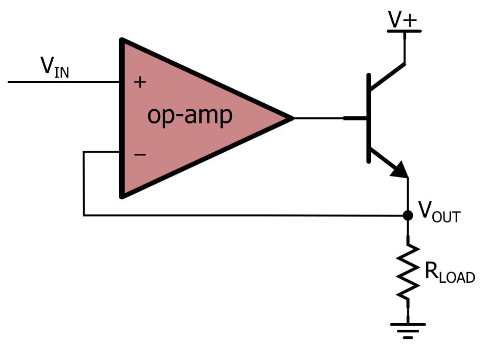
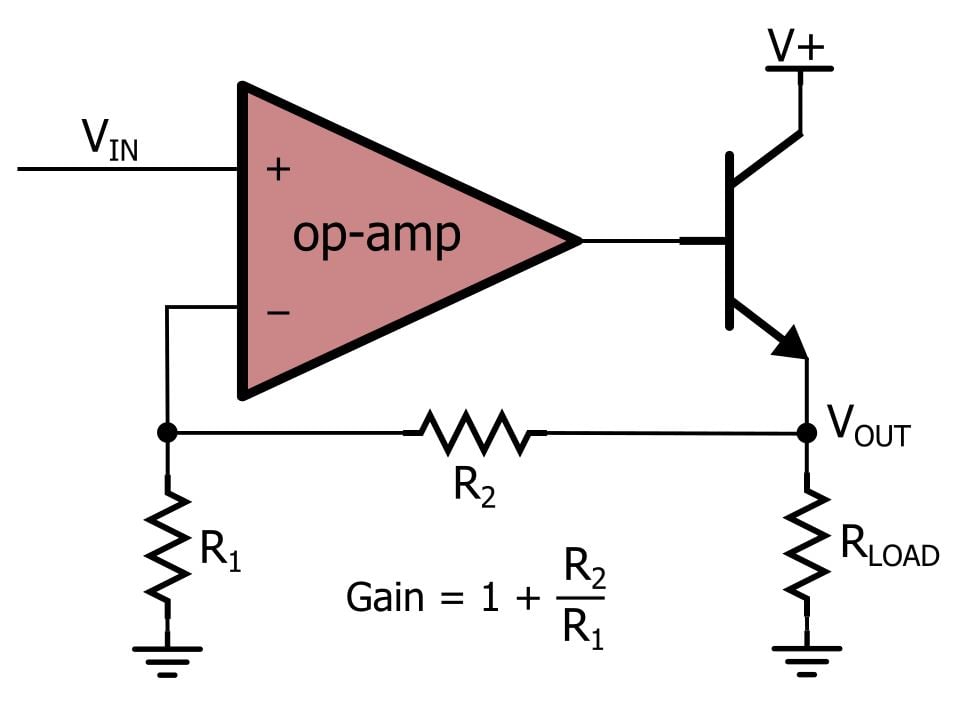
The most basic circuit for buffering an op-amp’s output current is the following:
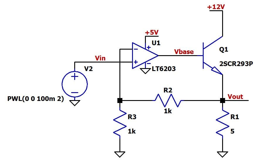
And here is a corresponding LTspice schematic:
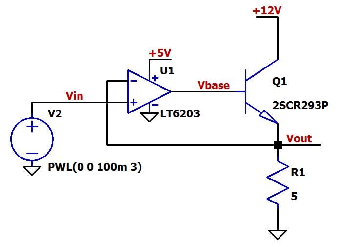
Let’s get a solid conceptual understanding of this circuit before we move on. The input is applied to the noninverting op-amp terminal, and the output is connected directly to the base of the BJT. The op-amp and the BJT could use the same positive supply, but in this case, we are assuming that two voltages are available—a 5 V supply for low-power, low-noise circuitry, and 12 V for the high-power portion of the design. The value of the load resistor is very low, such that output voltages greater than about 200 mV applied directly to the load would require more output current than the LT6203 can provide. The transistor chosen in the LTspice schematic can handle about 1000 mA, which means it is good for load voltages up to 5 V.
The key to this circuit is the feedback connection. Remember the “virtual short”: when analyzing an op-amp in a negative-feedback configuration, we can assume that the voltage at the noninverting terminal equals the voltage at the inverting terminal. This alone tells us that the output voltage (i.e., the voltage across the load) will be equal to the input voltage. But let’s go a little deeper to make sure we actually understand what’s going on; the virtual short is sort of a superstition that can distract us from the reality of how an op-amp functions. The op-amp multiplies the differential input voltage by a very large gain. Thus, with negative feedback, the op-amp rapidly reaches equilibrium because the large changes in output voltage reduce the differential voltage that is causing these very output changes. In this equilibrium state, the output has stabilized at whatever voltage eliminates the difference between the voltages at the inverting and noninverting input terminals—in other words, the op-amp automatically adjusts its output in whatever way is needed to make VIN– equal to VIN+.
In the context of this output-buffering circuit, the op-amp automatically generates whatever output voltage is needed to make the BJT’s emitter voltage equal to the input voltage. Think how difficult this would be in an open-loop situation—somehow the amplifier’s input-to-output relationship would have to be designed to compensate for the BJT’s base-to-emitter voltage drop, which is neither linear nor predictable. But with an op-amp plus some negative feedback, the problem becomes trivial.
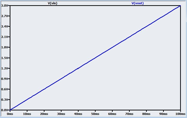
Let’s reinforce this conceptual understanding with a couple simulations. The first is not very exciting; it simply confirms that the output voltage tracks the input voltage (the VIN trace is hidden underneath the VOUT trace):
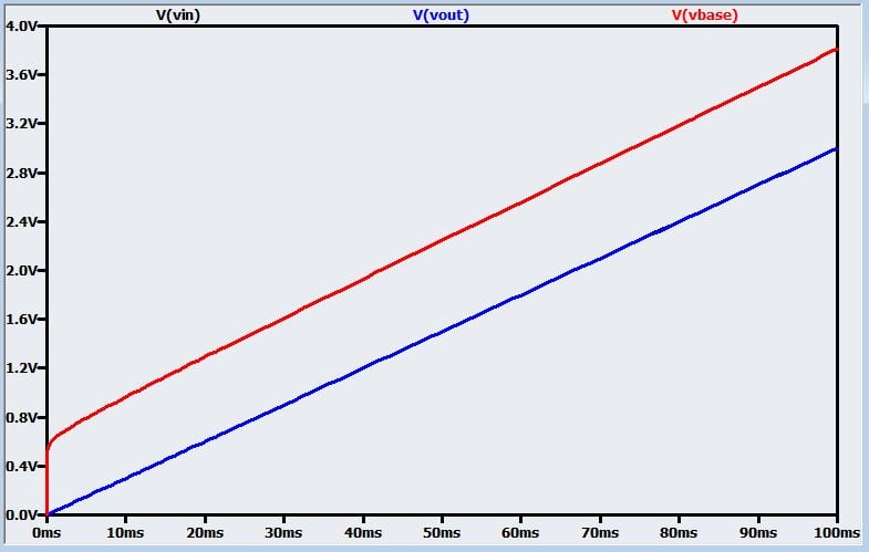
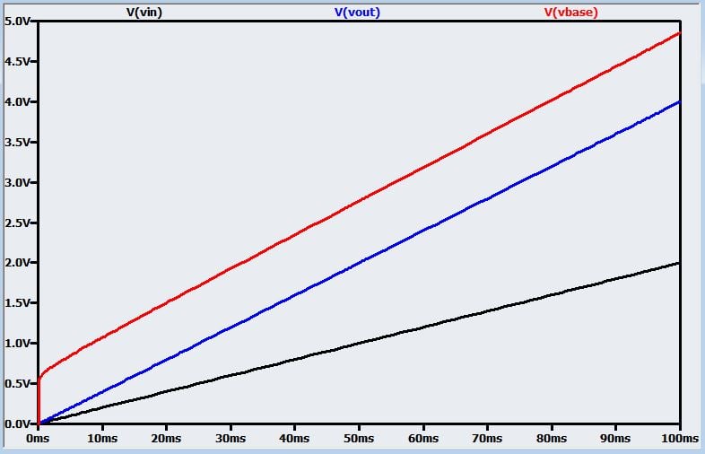
This next plot shows what the op-amp output terminal must do to produce the proper voltage across the load.
Adding Gain
This basic circuit is not limited to the unity-gain configuration. As with a non-buffered op-amp, you can insert resistors into the feedback path to create overall gain from the input to the load voltage. Here is the non-unity-gain version of the circuit:
And here is the new LTspice schematic, followed by a plot with VIN, VOUT, and the voltage applied to the base of the BJT.
Simple, but Not Foolproof
With a reliable, straightforward circuit like this, there is always the risk of complacency. Here are some potential problems you need to keep in mind:
- This is an obvious one, but make sure the BJT can handle your load current. For example, a 2N2222 transistor that you find among your spare parts is probably rated for only 800 mA of continuous collector current.
- This one is not so obvious: Are you exceeding the transistor’s maximum power dissipation? This issue is particularly elusive because it’s the sort of thing you might not notice in a simulation—for example, the simulations performed in this article did little to warn us that we were burning up the 2SCR293P transistor. The maximum power dissipation for this part with “each terminal mounted on a reference land” (I’m not quite sure what that means) is 0.5 W. In our circuit, if VOUT = 3 V, the current through the load is (3 V)/(5 Ω) = 600 mA and the transistor’s collector-to-emitter voltage is 12 V – 3 V = 9 V. Thus, the power dissipation is about (600 mA) × (9 V) = 5.4 W. So the collector current is well within the acceptable range, but we have exceeded the maximum power by a factor of 10! You can help to remedy this by using a lower supply voltage if possible, and after that, you need to choose a higher-power transistor.
- When the BJT is operating in the active region, the current flowing into the base is approximately equal to the load current divided by beta, otherwise known as hFE or the DC current gain. Thus, the op-amp still needs to supply some current, and you might run into trouble if you have high load current combined with a relatively puny op-amp output stage. For example, if your load current is 2500 mA and you are using a transistor with hFE = 100, you will need about 25 mA of base current; some op-amps are not capable of this.
- Keep in mind that the op-amp’s output voltage is about 0.7–0.9 V higher than the load voltage. You have to take this into account when choosing the op-amp’s supply voltage. For example, let’s say you need a load voltage range of 0 to 4 V; is a 5 V supply adequate? Maybe not: the base voltage might need to go as high as 4.9 V, and if the op-amp’s output swing is limited to the positive rail minus 0.8 V, you will have a problem.
- The BJT will start to enter saturation when the base voltage exceeds the collector voltage by about 0.5 V, and since the base voltage is about 0.7–0.9 V above the load voltage, the BJT’s collector voltage (which in this circuit is the same as the supply voltage) needs to be at least 0.9 V – 0.5 V = 0.4 V higher than the maximum required load voltage. (These numbers are approximate and will vary based on operating conditions and the transistor’s electrical characteristics.) BJT saturation will cause the load voltage to level out before it reaches the BJT supply voltage.
Conclusion
I think we have covered this op-amp current-buffering circuit in adequate detail. In the next article we will look at variations on this circuit that make it compatible with a wider variety of applications.
Next Article in Series: How to Buffer an Op-Amp Output for Higher Current, Part 2


The LT6203 has a push-pull output that can source and sink current. The circuit in this article only has the ability to source current.Will future articles have circuits that can source and sink current?
The LT6203 is also a rail-to-rail input and output op-amp. Adding a buffer transistor eliminates the rail-to-rail output capability. I understand it’s a trade-off between power and output swing, so maybe choosing a rail-to-rail op-amp is the best choice for this circuit.
What impact does buffering the output of the LT6203 have on precision op-amp circuits, where an error budget might be a few mV or less.
What impact does buffering the output have on low-noise applications.
Why did you choose to buffer the output with a BJT vs a MOSFET? A MOSFET gate will require less current, which might be good for a low power op-amp like the LT6203. Maybe it doesn’t matter much if the current gain of the transistor is high enough. I guess the BJT might give the circuit a wider output swing as the emitter forward drop is often less than gate threshold voltage of a MOSFET.