
Learn LabVIEW FPGA on NI myRIO - Hello World!
Learn LabVIEW FPGA by programming the on-board Xilinx FPGA of the student-focused embedded device NI myRIO.
Related Articles
Utilising LabVIEW FPGA on NI myRIO:
Part 1: What is LabVIEW FPGA
Part 2: Hello World (Blinking an LED)
Part 3: Reading Analog Values
Part 4: FIFOs
Part 5: 3rd-party Code
Overview
This is Part 2 of the Utilising LabVIEW FPGA on NI myRIO article series. In the last article we covered the basics of what an FPGA is, how to create a LabVIEW project, how to access the myRIO embedded device, and we even wrote our first FPGA application. This article will show how to utilise what we just learned to interface with the real world. It will explain how to access the Digital Input and Output ports of the myRIO and how to use data from previous code loop iterations using a concept in LabVIEW called Shift Registers. Then we will connect a simple Light-Emitting Diode to one of the Digital Lines of the myRIO and make it blink by turning it on and off every second.
Wiring the Hardware
First we will need a Light-Emitting Diode (LED) to switch. It is recommended that you use a 3.3V LED as the myRIO is only capable of providing 3.3 Volts on the Digital Lines. As we will see in later articles, when it comes to reading it will be able to go further. Note that a regular 5V LED would also work but might not be as bright. Then we need to calculate a value for our current-limiting resistor that will be connected in series between the LED and the Digital Line. This is needed because Light-Emitting Diodes are very sensitive and without a resistor to limit the current, it would essentially "short" the digital line and the ground of the myRIO. While it would not necesserily break the myRIO, it could easily blow the LED. Not to mention that ignoring the current-limiting resistor is considered a bad wiring practise overall. There is a lot of fantastic material on the topic available online and we will not dwell too much into the theory. Looking at the wiring schematic (Figure 1) we can see that the Resistance, R can be found as follows:

Where Vs is the source voltage, in our case 3.3V. Vf is the forward voltage of an LED, usually specified in the datasheet, in our case 1.4V. Finally i is the current needed to drive the LED to full brightness. This value can also be found in most datasheets and usually is around 20-30 mA. Substituting these numbers into our equation we find that the recommended series resistor value to limit the current flowing through the LED is between 60 and 95 Ohms. In the time of writing this article, the closest resistor value I was able to find was 330 Ohms and it worked fine. As a rule of thumb, it is better to reduce more current than less. Saying that, with resistances over 1 KOhm you would likely lose most of the brightness of the component, but there is surely some flexibility. As it shows in Figure 1 and 2, for the purposes of this tutorial we will use Digital Line 0 of the Port C of the myRIO.

Figure 1 Circuit Diagram

Figure 2 The 330Ohm resistor was twised around the Anode of the LED and connections to the myRIO were established using two female-to-female jumper wires.
Writing the FPGA Code
Just like in the first article, let's create a new LabVIEW project, save it as "myRIO FPGA Series 2.lvproj" and add the NI myRIO as the target device. Then we will need to create a new VI and save it within the same directory as "FPGA.VI". Within this VI we need to create a while loop (A) to make sure our code runs continuously. Like last time, we will wire a False boolean constant to the stop condition terminal (B) to make sure our code never stops executing. Then we need to drag and drop the DIO0 resource from Port C of the project (C) to our FPGA VI, as shown in Figure 3. By default it will be in read state so make sure to right-click on the DIO0 resource and select "Change to Write". Then we create another boolean constant that we will invert each loop iteration (D). To keep the value from previous loop iteration we will make use of Shift Registers (E). Imagine a Shift Register as a memory block that "remembers" what was wired to it the last time it ran. To add a Shift Register, first wire the data through to the while loop, then right-click on the terminal and select "Replace with Shift Register...". This way we can now keep on inverting the value each time the while loop runs, hence turning the LED on and off. Then we should add some timing (F), otherwise our code will keep switching the LED way too fast for us to see! Make sure the timing is configured to miliseconds by double-clicking on the timing function and selecting "Counter Units" to "mSec" (G). Finally we can also create an indicator to double-check that our inverting logic is actually working as expected (H).
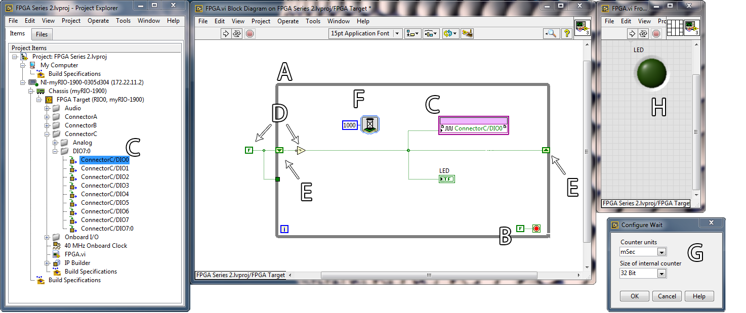
Figure 3 LabVIEW FPGA Code with accompanying explanations
Running the FPGA Code
If you have followed the tutorial correctly and ran the FPGA VI, after compilation you should now see both the LED indicator on the Front Panel and the actual LED blinking simultaneously. Congratulations, you have now successfully implemented Hardware I/O interfacing through FPGA in several easy steps using LabVIEW and the NI myRIO. You can try tweaking the timing value as shown in (F) of Figure 3 and see how that changes the frequency of the LED switching. Alternatively you can also try connecting the LED's Anode to another DIO line, changing the code and re-compiling to ensure you understand what the tutorial has covered.
In the next article we will cover how you can make this LED not only blinks, but also change brightness. Moreover you will be controlling this using a variable resistor known as potentiometer!
Next Article in Series: Reading Analog Values and PWM with LabVIEW FPGA


i cant find the link to the 4th and 5th article of this series. please help asap