Thermal Design with Linear Voltage Regulators
Will your linear regulator function properly under all possible operating conditions? To find out, you need to understand power dissipation and thermal resistance.
Will your linear regulator function properly under all possible operating conditions? To find out, you need to understand power dissipation and thermal resistance.
Supporting Information
Designer Beware
At first glance, linear voltage regulators seem so simple. The part’s datasheet indicates the maximum input voltage, the maximum output current, and the output voltage (if the output is fixed rather than variable). If your design requirements are a little more demanding, you might also check the accuracy of the output voltage, the dropout voltage, the output noise, and the operating ambient temperature range. If all these specs look good, you can drop in the part and everything will be fine, right? Well, most of the time, yes, everything will be fine, but it’s also possible that the design will thoroughly fail.
Current vs. Power
The first thing to understand is that the part’s maximum output current is not an isolated specification. Output current influences power dissipation, and power dissipation influences junction temperature, and if the junction temperature gets too high, the part will cease to function properly. Permanent damage is a possibility, though most (maybe all) modern linear regulators incorporate thermal protection circuitry that will simply limit the output current in an attempt to reduce the internal temperature. In either case, your design will malfunction; even worse, it may malfunction in a strange or intermittent way, leading to potentially high levels of troubleshooting-induced frustration. The best remedy, as usual, is prevention.
The Two Temperatures
When confirming that a particular component is compatible with a system’s temperature requirements, we generally look at the operating ambient temperature range listed in the part’s datasheet. This is adequate for most situations, but it is nonetheless rather imprecise. Strictly speaking, the ambient temperature does not determine whether the part will function properly, just as the outdoor air temperature does not directly determine whether you are comfortable inside your house. What really matters is the internal temperature, i.e., the temperature experienced by the semiconductors—after all, it’s the transistors that make a voltage regulator regulate voltage, not the plastic package. This internal temperature is referred to as the junction temperature.
We can usually look at nothing more than the ambient temperature range because the junction temperature is often similar to the ambient temperature. If you live in a drafty wooden shack and cook outdoors over an open fire, the interior shack temperature won’t differ much from the outdoor temperature. This is simply thermal equilibrium at work. The same thing happens with many electronic components, because many electronic components do not dissipate significant amounts of power. This is the critical point. Sensors, data converters, microcontrollers, logic gates, and so forth tend to dissipate modest amounts of power, and consequently the junction temperature does not greatly differ from the ambient temperature. But linear voltage regulators are a different story. Imagine if you were baking bread in that wooden shack—all day long. That’s more or less what the voltage regulator is doing, and the result is a junction temperature that can significantly exceed the ambient temperature. Consequently, one key to robust linear-regulator design is ensuring that the junction temperature stays within the acceptable range even during worst-case operating conditions.
First, Calculate Power
The two factors that determine the difference between ambient temperature and junction temperature are power dissipation and thermal resistance. First let’s look at power dissipation.
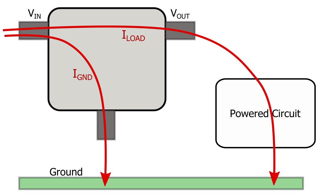
This diagram shows the two current paths in a linear regulator; the path from the input pin directly to ground is called the ground current (IGND), and the path from the input pin to ground through the powered circuit is the load current (ILOAD). The internal power dissipation resulting from these two currents are
\[P_{I_{GND}}\ \ =I_{GND}\times V_{IN}\ \ \ \ \ \ \ \ \ \ \ P_{I_{LOAD}}\ \ \ =I_{LOAD}\times\left(V_{IN}-V_{OUT}\right)\]
Thus, the total power dissipation inside the regulator is the following:
\[P_{TOTAL}=\left(I_{GND}\times V_{IN}\right)+\left(I_{LOAD}\times\left(V_{IN}-V_{OUT}\right)\right)\]
The ground current—i.e., the current consumed by the regulator’s internal circuitry in the process of generating a regulated output voltage—will generally be much smaller than the load current. So if you don’t feel like checking the ground current specs, you can simply ignore this term and the result should be pretty close.
Thermal Resistance
The power dissipated inside the regulator leads to a persistent difference between the junction temperature and the ambient temperature. So we know that the internal circuitry of the regulator will always be hotter than the surrounding environment; the question is, how much hotter? This is where thermal resistance comes into play. As the name implies, this quantity corresponds to how much the flow of heat is resisted. In the context of regulator design, higher thermal resistance means that there is more resistance to the heat that wants to flow from inside the regular to the surrounding environment. Higher resistance means less heat flow, and less heat flow means a larger steady-state temperature difference. This relationship is reflected in the following equation, where thermal resistance is denoted by θ and has units of °C/watt.
\[\Delta T_{JA}=P_{TOTAL}\times\theta_{JA}\]
So if you know the regulator’s power dissipation (PTOTAL) and the thermal resistance from the internal circuitry to the ambient environment (θJA), you can calculate the difference between the ambient temperature and the junction temperature (ΔTJA). Unfortunately, determining θJA is not exactly straightforward.
The first thing to understand is that θJA is not a fixed quantity. It depends on your PCB design. Actually, this is a critical point: you cannot assume that the ambient temperature range given in the regulator’s datasheet is valid for all PCB layouts. In other words, if you subject the regulator to maximum input voltage and maximum output current, a high-thermal-resistance PCB layout could cause the part to overheat, even if the ambient temperature remains in the acceptable range.
Careful Thermal Design Can Be Crucial!
Let’s work through an example to demonstrate the importance of considering thermal resistance in your regulator designs. This example is based on the ADP3338 low-dropout voltage regulator from Analog Devices. The relevant specs are as follows:
|
Maximum load current |
1000 mA |
|
Maximum ground current |
30 mA |
|
Output voltage |
3.3 V |
|
Maximum input voltage |
8 V |
|
Maximum junction temperature |
150°C |
|
Maximum ambient temperature |
85°C |
So first we need to answer the following question: If the device is subjected to worst-case operating conditions, how low must the thermal resistance be? We can rearrange the above equation as follows:
\[\theta_{JA}=\frac{\Delta T_{JA}}{P_{TOTAL}}\]
Inserting the appropriate values, we get the following:
\[\theta_{JA}=\frac{\left(150^{\circ}C-85^{\circ}C\right)}{\left(.03\ A\times8\ V\right)+\left(1\ A\times\left(8\ V-3.3\ V\right)\right)}=\frac{65^{\circ}C}{4.94\ W}=13.2\ \frac{^{\circ}C}{W}\]
So far so good . . . except that a thermal resistance this low is impossible! Consider the following diagram from the ADP3338 datasheet:
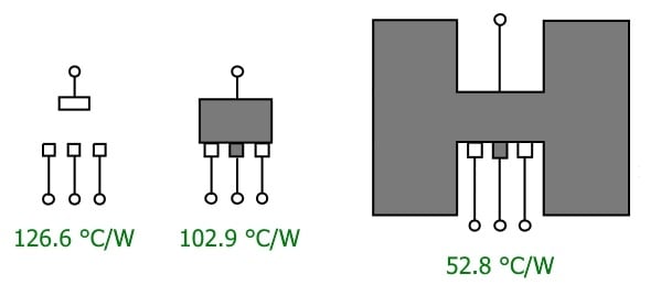
This diagram is intended to give you an idea of what thermal resistance to expect from different PCB layouts. So if you just solder this regulator to your board without providing any extra copper to help dissipate heat, the thermal resistance will be about ten times too high. Even the layout on the far right, which incorporates a generous copper pad, is still much higher than the 13.2 °C/W needed for worst-case operation. You can further reduce the thermal resistance by expanding the copper area and using numerous vias to provide a thermal path to other PCB layers, but in this case, you will never reach 13.2 °C/W. This is because the junction-to-ambient thermal resistance is the sum of case-to-ambient thermal resistance (which depends on the layout) and junction-to-case thermal resistance (which depends only on the IC package), and the ADP3338’s junction-to-case thermal resistance is 26.8 °C/W—already twice as high as the overall thermal resistance needed for these worst-case operating conditions. Of course, this is an extreme example. In practice, you don’t push a part to its limits like this. Usually, the required thermal resistance is achievable, but you might need far more than the minimum amount of copper.
Conclusion
Proper thermal design for linear regulators is easy to overlook, because in many cases the operating conditions are so far from worst-case that the design will work even if thermal resistance never so much as enters your mind. But the process is actually fairly simple, and it could save your board from the infamy of failing at high ambient temperature. You just calculate worst-case power dissipation and then estimate thermal resistance as well as you can based on information in the datasheet (or the datasheet for a similar part). Then you can calculate the highest ambient temperature at which the device’s junction temperature will be below the specified maximum.