
How to Use Simple Converter Circuits
Different circuit connections are explored here. For instance, an inversion of source and load converts the buck converter into a boost converter, the cascade connection of the converters leads to the formation of the buck-boost, and the Cuk converter from the basic buck and boost converters.
Utilization of Simple Converter Circuits in the Derivation of Other Types of Converters.
Recommended Level
Beginner
In this technical article, different circuit connections are explored in which different types of converters are derived. For instance, an inversion of source and load converts the buck converter into a boost converter, the cascade connection of the converters leads to the formation of the buck-boost, and the Cuk converter from the basic buck and boost converters. Different connections of the load between the outputs of more than one converter can cause the formation of a single-phase or multi-phase inverters.
Inversion of Source and Load
Consider the simple buck converter shown in Fig.1.
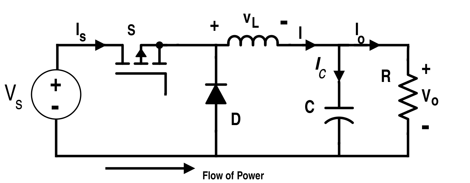
Figure 1. Circuit Diagram for Buck Converter
From the principle of volt-time balance criterion for inductor,
Conversion ratio of this circuit is,
$$\frac{V_{O}}{V_{S}}=D$$ [Equation 1]
Where D is the duty cycle ratio for the switch S i.e. $$D=\frac{T_{ON}}{T_{ON}+T_{OFF}}$$
Now, if we reverse the input and output ports as shown in Fig. 2. The capacitor remains intact with the load to bypass the high frequency ripples.
.png)
Figure 2. Buck Converter with Source and Load Inverted
As the Equation 1 also holds true for the inverted circuit, the conversion ratio will be:
$$\frac{V_{S}}{V_{O}}=D$$ or $$V_{O}=\frac{1}{D}V_{S}.$$
Here, load is connected to the supply when S is on. But the direction of the “flow of power" is reversed as shown. If we interchange the position of two switches S and D, we will get the following configuration of converter as shown in Fig.3. Fig. 3 configuration is more preferable as time for charging of the inductor is under control through switch S.
.png)
Figure 3. Inversion of Source and Load with S and D Interchanged
Since the switch S is in exchange of the position of D, then it needs to be kept on when it was off in the Fig. 2 and kept off when it was on with respect to the configuration shown in Fig.2. The duty cycle for this case will be 1-D. Thus, $$V_{O}=\frac{1}{1-D}V_{S}.$$ The load here is connected to the supply when switch S is off. This configuration shown in Fig.3 is similar to the boost converter.
Cascaded Connection of Converters
Let there be two converters with conversion ratios C1 and C2. If they are connected in a cascade manner and have the same duty cycle ratio for the converter switch, then overall conversion ratio will be C1 X C2.
Let the first converter be a buck converter and the second one is boost; and they are connected in cascade as shown in Fig. 4.
This converter is non-inverting, i.e. if the input voltage is positive polarity than output voltage is also of positive polarity.
.png)
Figure 4. Cascaded Buck and Boost Converter
Clearly, capacitor CA can be removed while inductors LA and LB can be combined as shown in Fig. 5 to serve the same purpose seen in Fig.4.
.png)
Figure 5. Non-Inverting Buck-Boost Converter
In steady state, cascade connection conversion ratio for the buck-boost converter is the product of conversion factor for the buck converter and boost converter. Conversion ratio $$=\frac{V_{O}}{V_{S}}=D\, X\,(\frac{1}{1-D})$$ where 0 < D < 1.
Output voltage is less than the input voltage if D<0.5 and the output voltage is greater than the input voltage if D>0.5.
This circuit can further be simplified by reducing the number of switches but it will reverse the polarity of output voltage. This occurs due to the reversal of the polarity of the inductor during the one sub-interval. Its configuration is shown in Fig.6.
.png)
Figure 6. Inverting Buck-Boost Converter
Thus, the conversion ratio for the inverting buck-boost converter is,
$$\frac{V_{O}}{V_{S}}=-\frac{D}{1-D}$$
Similarly, Cuk converter can be obtained by cascading the boost converter followed by the buck converter as shown in Fig. 7. The Cuk converter is more beneficial as it has the ripple-free input current feature of boost converter and the ripple-free output current feature of the buck converter.
.png)
Figure 7. Boost-Buck Converter
The circuit shown in Fig. 7 can be further simplified to Fig. 8 as shown. Conversion ratio for this converter is the same as of the buck-boost converter.
.png)
Figure 8. Ćuk Converter
Rotation of Three-Terminal Cells
Consider the basic buck, boost, buck-boost and the Ćuk converter circuits again as shown in Fig. 9.
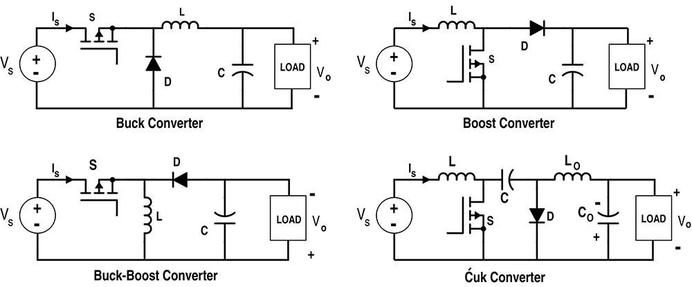
Figure 9. Basic Converters
Switch-and-inductor combination or switch-and-capacitor combination can form three-terminal cells which can be used to realize the entire basic converter configurations shown in Fig.9. These terminal cell configurations consist of a single-pole double-throw switch which when rotated shows the above configuration of converters as given in Fig. 10 and 11.
.png)
Figure 10. Three-Terminal Cell Configuration (Inductor with SPDT Switch)
Clearly, if the terminals of the three-terminal cell (1, 2, 3) are connected in the following fashions, respective converters can be realized as mentioned below.
1-------- (A), 2 ------(B), 3---------(C) ➔ Buck Converter
1---------(C), 2-------(A), 3---------(B) ➔ Boost Converter
1---------(A), 2-------(C), 3--------(B) ➔ Inverting Buck-Boost Converter
Similarly, another configuration of three-terminal cell formed by the combination of switch and capacitor as shown in Fig.11.
.png)
Figure 11. Three-Terminal Cell Configuration (Using Capacitor and Switch)
The three-terminal cell can be rotated to connect the following terminals to realize the following converter configurations.
1-----------(A), 2------------(B), 3-------------(C) ➔ Buck Converter.
1-----------(C), 2 -----------(A), 3-------------(B) ➔ Boost Converter
1-----------(A), 2------------(C), 3-------------(B) ➔ Ćuk Converter
Differential Connection of the Load
Converters alone that are in cascade combination can only produce the unipolar voltage. In the case of the inverter, the bipolar voltage is required. This bipolar voltage can be attained with the help of differential connection of the basic converters.
The differential connection of two buck converters is shown in Fig.12.
.png)
Figure 12. Differential Connection of Two Buck Converters
The output voltage for the differential connection is,
$$V_{O}=V_{A}-V_{B}$$
This Fig. 12 can further be simplified by eliminating one of the capacitors as shown in Fig. 13.
.png)
Figure 13. Simplified Differential Connection of Buck Converters
If switch SA has a duty cycle D, the duty cycle for switch SB must be (1-D).
Thus, $$V_{O}=DV_{S}-(1-D)V_{S}$$
$$\Rightarrow V_{O}=(2D-1)V_{S}.$$
When D < 0.5 ➔ VO is negative,
And when D > 0.5 ➔ VO is positive.
Three-phase inverter can also be obtained with the configuration pattern shown in Fig. 14.
.png)
Figure 14. Differential Connection to Derive Three-Phase Inverter Configuration


Hello, one question: Why can the capacitor Ca be removed? I understand that the voltage is kept the same but doesn’t it affect current? Thanks
Hi,
Why is the P mosfet plugged in the other way, Be aware there is a diode on most mosfet’s that allow current to flow either on or off if plugged in wrong way