
(a) Crystal radio. (b) Modulated RF at antenna. (c) Rectified RF at diode cathode, without C2 filter capacitor. (d) Demodulated audio to headphones.
An antenna ground system, tank circuit, peak detector, and headphones are the main components of a crystal radio seen in figure (a). The antenna absorbs transmitted radio signals (b) which flow to ground via the other components. The combination of C1 and L1 comprises a resonant circuit, referred to as a tank circuit. Its purpose is to select one out of many available radio signals. The variable capacitor C1 allows for tuning to the various signals. The diode passes the positive half cycles of the RF, removing the negative half cycles (c). C2 is sized to filter the radio frequencies from the RF envelope (c), passing audio frequencies (d) to the headset. Note that no power supply is required for a crystal radio. A germanium diode, which has a lower forward voltage drop, provides greater sensitivity than a silicon diode.
While 2000Ω magnetic headphones are shown above, a ceramic earphone, sometimes called a crystal earphone, is more sensitive. The ceramic earphone is desirable for all but the strongest radio signals.
The circuit in the figure below produces a stronger output than the crystal detector. Since the transistor is not biased in the linear region (no base bias resistor), it only conducts for positive half cycles of RF input, detecting the audio modulation. An advantage of a transistor detector is amplification in addition to detection. This more powerful circuit can readily drive 2000Ω magnetic headphones. Note the transistor is a germanium PNP device. This is probably more sensitive, due to the lower 0.2V VBE, compared with silicon. However, a silicon device should still work. Reverse battery polarity for NPN silicon devices.

TR One, one transistor radio. No-bias-resistor causes operation as a detector
The 2000Ω headphones are no longer a widely available item. However, the low impedance earbuds commonly used with portable audio equipment may be substituted when paired with a suitable audio transformer.
The circuit in the figure below adds an audio amplifier to the crystal detector for greater headphone volume. The original circuit used a germanium diode and transistor. A schottky diode may be substituted for the germanium diode. A silicon transistor may be used if the base-bias resistor is changed according to the table.
![]()
Crystal radio with one transistor audio amplifier, base-bias
For more crystal radio circuits, simple one-transistor radios, and more advanced low transistor count radios.
Regency TR1: First mass produced transistor radio, 1954
The circuit in the figure below is an integrated circuit AM radio containing all the active radio frequency circuitry within a single IC. All capacitors and inductors, along with a few resistors, are external to the IC. The 370 pF variable capacitor tunes the desired RF signal. The 320 pF variable capacitor tunes the local oscillator 455 KHz above the RF input signal. The RF signal and local oscillator frequencies mix producing the sum and difference of the two at pin 15. The external 455 KHz ceramic filter between pins 15 and 12, selects the 455 KHz difference frequency. Most of the amplification is in the intermediate frequency (IF) amplifier between pins 12 and 7. A diode at pin 7 recovers audio from the IF. Some automatic gain control (AGC) is recovered and filtered to DC and fed back into pin 9.

IC radio
Figure below shows conventional mechanical tuning (a) of the RF input tuner and the local oscillator with varactor diode tuning (b). The meshed plates of a dual variable capacitor make for a bulky component. It is economic to replace it with varicap tuning diodes. Increasing the reverse bias Vtune decreases capacitance which increases frequency. Vtune could be produced by a potentiometer.

IC radio comparison of (a) mechanical tuning to (b) electronic varicap diode tuning.
Figure below shows an even lower parts count AM radio. Sony engineers have included the intermediate frequency (IF) bandpass filter within the 8-pin IC. This eliminates external IF transformers and an IF ceramic filter. L-C tuning components are still required for the radio frequency (RF) input and the local oscillator. Though, the variable capacitors could be replaced by varicap tuning diodes.

Compact IC radio eliminates external IF filters
Figure below shows a low-parts-count FM radio based on a TDA7021T integrated circuit by NXP Wireless. The bulky external IF filter transformers have been replaced by R-C filters. The resistors are integrated, while the capacitors are external. This circuit has been simplified from Figure 5 in the NXP Datasheet. See Figure 5 or 8 of the datasheet for the omitted signal strength circuit. The simple tuning circuit is from the Figure 5 Test Circuit. Figure 8 has a more elaborate tuner. Datasheet Figure 8 shows a stereo FM radio with an audio amplifier for driving a speaker.

IC FM radio, signal strength circuit not shown
For a construction project, the simplified FM Radio in the figure above is recommended. For the 56nH inductor, wind 8 turns of #22 AWG bare wire or magnet wire on a 0.125 inch drill bit or other mandrel. Remove the mandrel and stretch to the 0.6-inch length. The tuning capacitor may be a miniature trimmer capacitor.
Figure below is an example of a common-base (CB) RF amplifier. It is a good illustration because it looks like a CB for lack of a bias network. Since there is no bias, this is a class C amplifier. The transistor conducts for less than 180° of the input signal because at least 0.7 V bias would be required for 180° class B. The common-base configuration has higher power gain at high RF frequencies than common-emitter. This is a power amplifier (3/4 W) as opposed to a small signal amplifier. The input and output π-networks match the emitter and collector to the 50 Ω input and output coaxial terminations, respectively. The output π-network also helps filter harmonics generated by the class C amplifier. Though, more sections would likely be required by modern radiated emissions standards.

Class C common-base 750 mW RF power amplifier. L1 = #10 Cu wire 1/2 turn, 5/8 in. ID by 3/4 in. high. L2 = #14 tinned Cu wire 1 1/2 turns, 1/2 in. ID by 1/3 in. spacing.
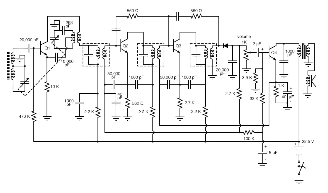
An example of a high gain common-base RF amplifier is shown in figure below. The common-base circuit can be pushed to a higher frequency than other configurations. This is a common base configuration because the transistor bases are grounded for AC by 1000 pF capacitors. The capacitors are necessary (unlike the class C, previous figure) to allow the 1KΩ-4KΩ voltage divider to bias the transistor base for class A operation. The 500Ω resistors are emitter bias resistors. They stabilize the collector current. The 850Ω resistors are collector DC loads. The three stage amplifier provides an overall gain of 38 dB at 100 MHz with a 9 MHz bandwidth.

Class A common-base small-signal high gain amplifier
A cascode amplifier has a wide bandwidth like a common-base amplifier and a moderately high input impedance like a common emitter arrangement. The biasing for this cascode amplifier (figure below) is worked out in an example problem Ch 4 .

Class A cascode small-signal high gain amplifier
This circuit is simulated in the “Cascode” section of the BJT chapter Ch 4 . Use RF or microwave transistors for best high frequency response.
![]()
PIN diode T/R switch disconnects receiver from antenna during transmit

PIN diode antenna switch for direction finder receiver

PIN diode attenuator: PIN diodes function as voltage variable resistors
The PIN diodes are arranged in a π-attenuator network. The anti-series diodes cancel some harmonic distortion compared with a single series diode. The fixed 1.25 V supply forward biases the parallel diodes, which not only conducting DC current from ground via the resistors, but also conduct RF to ground through the diodes’ capacitors. The control voltage, Vcontrol, increases current through the parallel diodes as it increases. This decreases the resistance and attenuation, passing more RF from input to output. Attenuation is about 3 dB at Vcontrol= 5 V. Attenuation is 40 dB at Vcontrol = 1 V with flat frequency response to 2 gHz. At Vcontrol= 0.5 V, attenuation is 80 dB at 10 MHz. However, the frequency response varies too much to use.
RELATED WORKSHEET:

In Partnership with Geehy Semiconductor

by Jake Hertz


by Jake Hertz


