Facebook
 Google
 GitHub
 Linkedin
2D Semiconductors May Be Key to 3D Integration, Say Stanford Researchers
New research indicates how 2D semiconductors could advance monolithic 3D integration in a scalable way—prolonging Moore's law in the process.
“Finding good metal contacts to semiconductors is a problem as old as semiconductors themselves,” said researcher Aravindh Kumar of Stanford University. “With every new semiconductor that is discovered (in our case, atomically-thin semiconductors like molybdenum disulfide (MoS2)), the problem of finding good contacts resurfaces again.”
The problem before Kumar and his fellow researchers, Katie Neilson and Kirstin Schauble, was finding metal contacts with nearly zero contact resistance (RC). The alternative would be wasted voltage and power at the metal-semiconductor junctions when these materials are integrated into circuits, LEDs, or solar cells.
To address this challenge, these Stanford researchers recently developed a novel technique to make alloyed metal contacts on monolayer 2D semiconductors. The improved metal-semiconductor contact resistance on the 2D semiconductors, combined with transition metal dichalcogenides' (TMD) optical properties, may pave the way for next-generation logic and memory technologies.
The Promise of 2D-semiconductor Transistors
According to the researchers, 2D semiconductors hold promise for solving the problem of channel control in highly-scaled transistors: decreasing the size of the device also decreases the channel length. Interface defects (because of the small size of the transistor gate channel) causes the carrier mobility to degrade.
The researchers say transition metal dichalcogenides (TMDs) such as MoS2 are preferable materials for sub-10nm channel transistors because of their high mobility at extremely low thickness.

Section of a FET based on a monolayer MoS2 channel. Image used courtesy of EPFL
Speaking to All About Circuits, the researchers explained the precedence of their latest research:
A previous study in our group showed that metals with high melting points such as nickel (Ni) and palladium (Pd) caused damage when deposited on monolayer MoS2. Being a delicate three-atom-thick material, this severely degrades its electronic performance. Therefore, we and other groups tried metals with low melting points, such as indium (In) and tin (Sn), to see if they would reduce damage to MoS2. Raman spectroscopy showed that they in fact induce negligible damage on monolayer MoS2. In and Sn are very prone to oxidation, so we capped these low melting metal contacts with gold (Au) and found that these contacts performed very well.
Electrical Characteristics of Alloy Contacts
To prevent wasted electrical voltage and power, the researchers sought out metal contacts with close to no contact resistance (RC). Currently, the best-known contacts with the least RC in the market are silver/gold (Ag/Au), gold (Au), and tin (Sn).
The Stanford researchers successfully created In/Au and Sn/Au alloy contacts with a contact resistance as low as 190 ohm.µm and 270 ohm.µm, respectively.

RC comparison between best-reported contacts to monolayer MoS2. Image used courtesy of Kumar et al.
“I would say we came up with this alloying technique serendipitously,” the team explained. “Then, we focused on the alloying aspect because that would ensure both thermal and chemical stability of these contacts. In/Au alloys, for example, would have a higher melting point than pure In, which makes them more industry friendly for any subsequent processing in transistor fabrication.”
Striving for Scalability
The most challenging aspect of the research, according to the team, was getting these 2D semiconductor transistors to work reliably and reproducibly. “We were not just shooting for one-off ‘hero’ devices—that is, single transistors that behaved very well,” the researchers noted. “Instead, we wanted to demonstrate statistically-relevant improvements in contact resistance across an entire chip. So, while we had excellent hero devices in our initial experiments, the yield or success rate was low.”
_and_In_Au_(right).jpg)
ID vs. VGS of Sn/Au (left) and In/Au (right). Image used courtesy of Kumar et al.
As an example, the researchers posited that if they made 100 devices initially, only two or three of them would perform well. Over months of trial and error, the team tried to nail down a device fabrication process and the testing methodology to ensure they were creating reproducible chip-wide results.
In the early stages of the team's research, they could only achieve good electrical performance with transistors at only one to three atom-thick 2D channels. Because 2D TMDs are atomically thin by nature, they are grown at low temperatures to avoid melting metals often used for chip interconnects—a contrast to crystalline silicon.
While the researchers concede that silicon is “still the gold standard when it comes to high-performance logic transistors,” they expressed optimism about the future of 2D TMD transistors, which may be useful for stacking layers of logic and memory on top of the base silicon CMOS layer.
2D Semiconductors: A Key to 3D Integration?
There are many indications that the future of Moore’s law will be driven by stacking transistors in the form of 3D-integrated chips, which can mitigate the memory-bandwidth problem or the "memory wall." 3D-integrated chips may also revolutionize design and routing methodologies.
2D semiconductors may be a key solution for creating such 3D-integrated chips because they can be readily grown at low temperatures while keeping the electrical properties intact. Because high-resistance contacts have always been a roadblock to adopting 2D semiconductors, this research could be groundbreaking for creating good industrial-grade 2D semiconductors on a large scale.

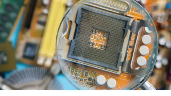
Pictured is a test structure that determines the contact resistance between a metal and a 2D semiconductor. Image used courtesy of Stanford University
The researchers elaborated, “If or when high-quality, low-temperature growths can be scaled up to 12” wafers, TMDs will play a role in memory and computing layers stacked on top of silicon logic. They could also play a role as access transistors in embedded DRAM, in the SRAM cache, or as 3D-Flash memory transistors.”
They added, “The first two examples benefit from lower off-state currents than are possible with silicon transistors because monolayer TMDs have larger energy band gaps than silicon.”
The Roadmap Ahead for 2D TMDs
In 2019, TSMC announced that it will start manufacturing SiGe as its PMOS channel material for 5nm technology. The research on Ge started around the early 2000s and it took almost 20 years for this study to reach the production units. 2D semiconductor research started around 2011 and has shown tremendous progress since then.
According to the Stanford researchers, it is fair to deduce from the Ge timeline that the 2D TMDs may appear in consumer electronics as early as 2030. However, some open challenges remain, like improving channel mobility and exploring P-type channel candidates. Until these issues are resolved, there is serious competition from other new 2D-semiconductor materials.
The continuation of Moore’s Law relies on new materials, device architectures, and solutions, the team said. “Because atomically-thin 2D materials (like MoS2) are one of the candidates for extending Moore’s Law, their contacts must be optimized in order for them to be suitable replacements or complements to silicon,” they assert. “Solutions for lower contact resistances, such as the alloyed contacts we proposed, allow for higher currents and better energy savings.”