Facebook
 Google
 GitHub
 Linkedin
UW Researchers Make Use of ‘Waste’ Heat With Thermophotovoltaic Device
The near-field device shows promise for harvesting energy from waste heat.
The University of Wisconsin (UW) College of Engineering recently developed and demonstrated a new type of device that converts heat directly to energy. The near-field thermophotovoltaic (TPV) device can be manufactured using standard semiconductor fab techniques for greater scalability.
Thermophotovoltaics convert heat into electricity, much like photovoltaics convert light into electricity. TPVs differ from conventional thermoelectric (TE) devices in that a TPV is a two-step/two-layer device. A thermophotovoltaic device has a top semiconductor layer that absorbs heat and, through tuned black-body radiation, emits infrared (IR) energy out the other side. A second semiconductor layer operates like a common photovoltaic (PV) cell and converts the IR photons into electricity.
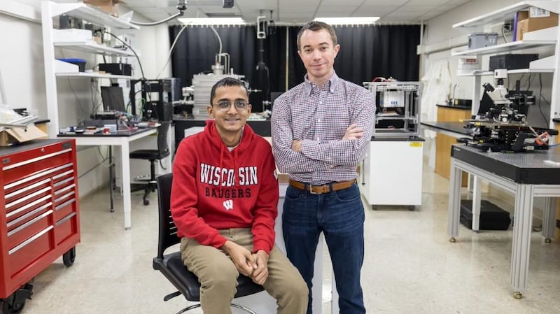
ECE graduate student Parth Solanki (left) and Assistant Professor Eric Tervo. Image used courtesy of University of Wisconsin College of Engineering
While thermophotovoltaic devices aren’t new, UW's prototype operates differently. Existing thermophotovoltaics have a relatively wide gap between the two layers. This means they operate with far-field infrared, which is not a dense form of energy. The new devices have a gap of just 150 nanometers and operate with near-field infrared. Near-field IR has a greater energy density than far-field.
UW's Thermophotovoltaic Architecture
As outlined in their paper published in Advanced Materials, UW's new TPVs are two-layer devices. The top layer, the emitter, is a semiconductor that absorbs heat and radiates infrared energy. The bottom layer is a different semiconductor that operates as a photovoltaic (PV) cell, converting the IR photons into electricity, as shown below.
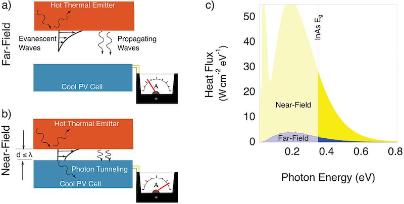
Block diagram of thermophotovoltaic devices and energy conversion curve. Image used courtesy of Wiley Online Library
The hot layer is positioned toward or connected to the heat source. It absorbs heat and re-radiates IR photons, as described by Planck's black body theory.
Decreasing the gap between the layers is one of the major innovations of the new devices. By bringing the layers closer, the PV cell can capture photons in the higher-density, near-field IR range. This increased efficiency makes the devices suitable for low-temperature operation.
The IR photon wavelength is the dividing line between near- and far-field for the purposes of this technology. With far-field TPV, the gap is greater than the wavelength. With existing devices, the gap has been substantially larger. A near-field has a gap that is less than the wavelength of the photons. The UW cell uses metalorganic vapor phase epitaxy semiconductor technology to grow a GaAs layer that is planar enough to have a 150-nm gap. The layer is grown thick and then etched, leaving pillars behind to create a gap when stacked on the indium arsenide (InAs) photovoltaic layer, as shown below.
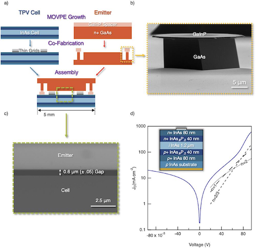
UW’s thermophotovoltaic call construction architecture. Image used courtesy of Wiley Online Library
Power Output and Scalability
The new TPV device generates 1.22 mW at 460°C—a 25x increase over a far-field TPV of the same size. The prototypes are still very small devices: 5 mm x 5 mm. Stacking the two layers with just a 150-nm gap is equivalent to stacking two football field-size sheets with a perfect 0.1-inch gap throughout. Such precision is necessary to keep the layers from touching and to avoid disturbing photon movement between the layers. With a near-field device, IR photons may bounce several times between the surfaces before being absorbed, increasing the power output.
The new TPV can be fabricated with conventional semiconductor manufacturing equipment, allowing for easy scaling once the design is satisfactory. The next step is to scale the devices up into the centimeter range. Along with scaling, the researchers plan to make the layers thinner and improve the emitter with silicon instead of GaAs. The thinner gap will improve the efficiency of the cell operation.
Leveraging Heat Byproduct
Eventually, the team hopes to achieve power up to 200 mW at 500 °C and heighten manufacturing precision to enable smaller gaps and improve the emitter material. Passive recovery of waste heat as electricity presents a big opportunity. Most devices in the modern world either operate on heat or generate heat as a byproduct of operation. Much of that heat is simply lost to the environment. UW's discovery shows promise for using that waste heat without needing exotic or expensive equipment.