
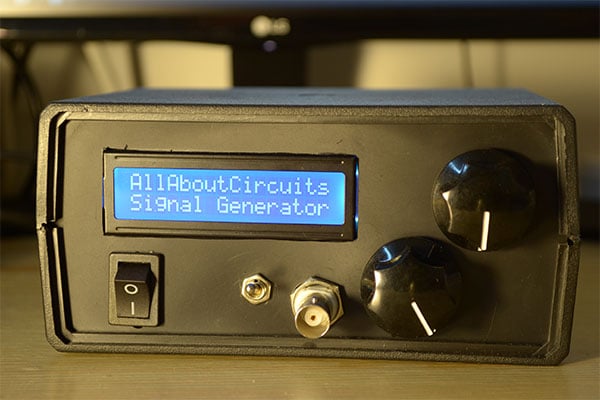
How to Build Your Own Function Generator Using Analog Devices’ AD9833
Tired of using your PC or mobile phone as a signal generator? It’s time to upgrade to a standalone one by making it yourself.
Learn how to make your own arbitrary waveform generator using an ATmega328p, a DDS function generator IC, an op-amp, a few passives, and some hard work.
Related Articles:
Having your own electronics laboratory at home is great—the only downside is that even basic equipment can be costly. Building your own devices is not only easier on your wallet, but it is also a great way to improve your knowledge. Therefore, in this article, I am going to explain how to build your own function generator.
What is a function generator?
First, a function generator (also called a tone generator) is an electronic device that can output a specific waveform at a set frequency. For example, one could generate a sinusoidal signal at 60Hz. You can use it to test the inner workings of audio amplifiers, find the characteristic of op-amps and diodes, make funky noises—the list of applications goes on.
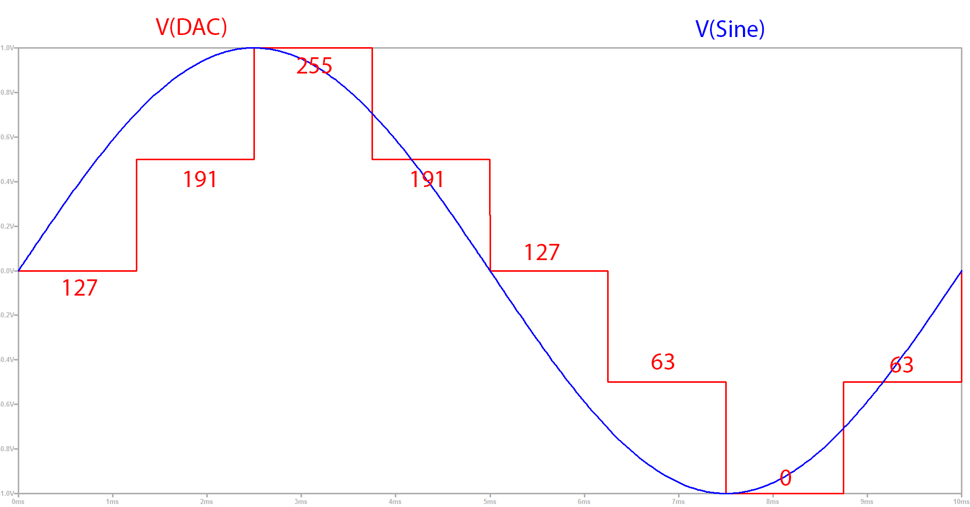
A DDS function generator is a digital arbitrary waveform generator, meaning it uses a digital-to-analog converter (DAC) to build a signal. It also has read only memory (ROM) where it stores amplitude values for specific waveforms at various time intervals based on a sampling frequency (Fs).
Let's say we have a DDS signal generator with an 8-bit DAC and it outputs a sinusoidal signal at 100Hz with a sampling frequency of 800Hz. Because the Fs is eight times the frequency of the sine wave, an engineer or, more likely, a computer needs to extract from a real sine wave eight amplitude values from t = 0 to t = 2π. This amplitude interval is [0, 255] (1111 1111 in binary = 255), which corresponds to the interval [-1, 1] with a real sine wave. As a picture is worth a thousand words, below is a comparison between the real sine wave and the one outputted by our imaginary (and low-performance) DDS function generator.
Building Your Own
The aim is to build a reliable function generator that can go up to 1MHz in frequency, up to 9V in amplitude, and that allows you to choose between sinusoidal, triangle, and clock (i.e., rectangular with 50% duty cycle) signals. To help you understand why I chose the components used, how they work together, and how the firmware was written, I am going to split this article into two big chunks, the hardware and the software.
Hardware
There are two main parts regarding the hardware aspect of this build: the power supply and the main PCB containing the function generator IC and the microcontroller.
The Power Supply
The main PCB will need two voltage rails: +12V and -12V. The symmetrical supplies are needed for the final amplification of the signal. A smaller +5V rail will be created directly on the main PCB by regulating the +12V one; it is needed to power the microcontroller, the AD9833, the function generator IC, and finally the 24MHz crystal oscillator. Below you can find the schematic of the power supply board:
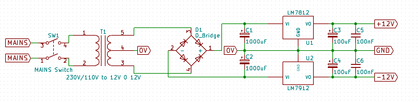
To obtain these voltages, a transformer will be used, from 230V or 110V (depending on your region) to two 12V AC lines (on the transformer it will usually be written something along the lines of 12V-0V-12V). An output current of 200mA is more than sufficient.
Remember that the output of a transformer is AC and we need DC. For this, we will be using a simple rectifier bridge. This will change the sinusoid into a positive signal. These usually come as standalone components but you can alternatively use four general purpose diodes such as 1N4001.
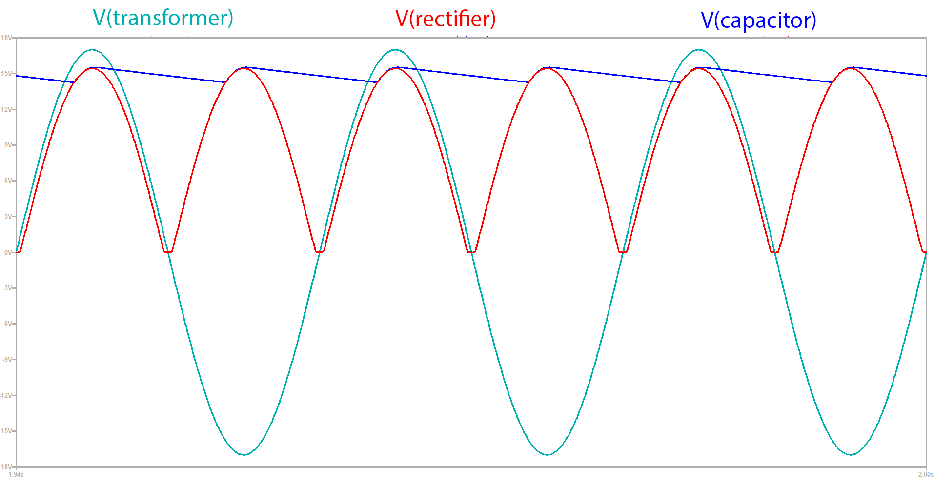
We will not be using it in the standard configuration as we want a symmetrical output, so we will connect them as in the schematic above: the ends of the transformer are connected to the rectifier, and the center tap is connected to ground. To smooth out the output we will first use two large capacitors, each 1000µF rated at 35V. Below you can find the output waveforms for the power supply rails at various stages:
In addition, to remove the ripple, two voltage regulators are used, the classic LM7812 and its sibling the LM7912, which is used for negative voltages. To top it off we add a 100µF capacitor and a 100nF one, both rated at 25V, to each regulator IC output. We want this supply to be as smooth as possible, as we will be using them to offset our final output voltage, and any AC components will propagate to the output.
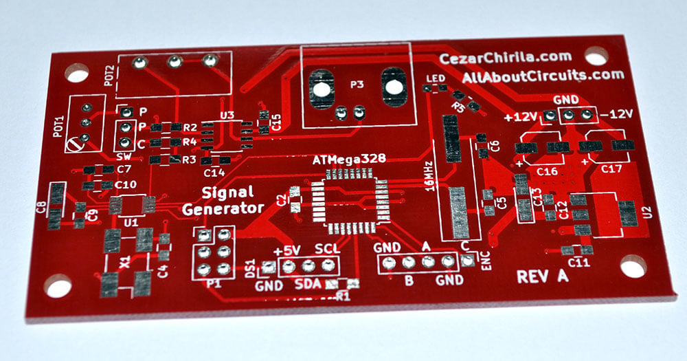
AD9833 Board
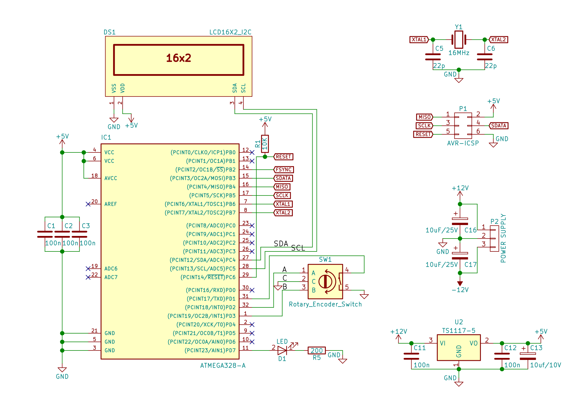
Let’s get to the main PCB. The LM1117-5V linear regulator is used to create a +5V rail from the +12V supply. To keep everything smooth, we add capacitors to both voltage input lines (+12V and -12V) and the output of the voltage regulator.
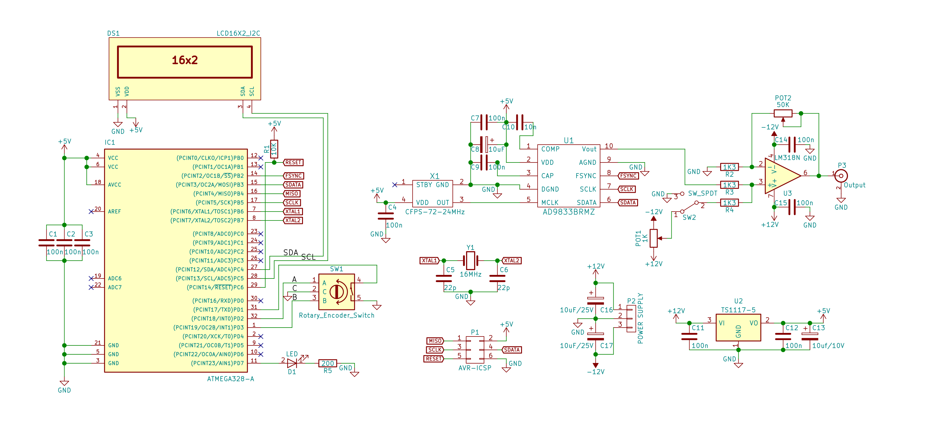
On the left side of the schematic, you will find an ATMega328p-AU microcontroller, the same used on the Arduino Uno but in an SMD package. To program the MCU, a 6-pin connector called AVR-ISP is placed next to it. It has two pins for power (+5V and GND) and four other pins for communication: MISO, MOSI, CLK, and RESET.
We will be using only one user input component, a rotary encoder with an integrated switch. This will be our control element to set the frequency, signal type, and other settings. The signals from the rotary encoder are routed to two interrupt pins on the microcontroller, PD2 and PD3 (D2 and D3 on the Uno), and the switch goes to an available pin that can act as an input; I chose PD1 (D1 on the Uno). We won’t be adding any pull-up resistors as we will be using the ones integrated into the microcontroller. Because mechanical contacts are not perfect, when we rotate the encoder, instead of an ideal pulse, a jittery signal will appear, but this can be easily fixed either by software or hardware using a capacitor. For the integrated switch, we will use the software method, and for the rotating contacts, two 100nF capacitors will be used.
A plain green LED is hooked up to pin PD7 (D7 on the Uno), for debugging purposes or to display status. The display used is a simple LCD with an HD44780 controller, which has 16 lines and two columns and includes a backlight. To reduce the number of connecting wires, an adapter board was used so that the only pins needed to control the LCD are 2 for data over I2C and another 2 for power (+5V and GND). The I2C lines on the microcontroller are on pins PC4 for SDA and PC5 for SCL. On the Arduino Uno, these are named A4 and A5, respectively.
Finally, the last connection for the microcontroller is made between it and the AD9833 integrated circuit. It uses a unidirectional SPI bus, meaning that data can only flow in one direction, from the MCU to the IC. The signals are MOSI (Master Out - Slave In), CLK (Clock), and CS (Chip Select, called FSYNC on the AD9833). To conclude the microcontroller portion, I should mention that decoupling capacitors with a value of 100nF are needed for each power supply pin.
Before continuing to the last part of the schematic, the part with the function generator IC, let me point out a few key features of the AD9833. Although I am going to sound like a salesperson, let’s start. It is a DDS type programmable waveform generator, so it takes a clock signal with a maximum frequency of 25MHz (for this particular IC), which it then divides based on a value passed by the microcontroller (maximum 228) via the SPI bus, and using a 10-bit DAC it outputs a waveform chosen by the microcontroller. The output has a peak-to-peak value of 0.65V-0.038V (VOUT maximum – VOUT minimum), and it has an offset of (0.65V-0.038V)/2. This means that VOUT minimum is very close to 0V. One important note is that the clock output (rectangular signal) has an amplitude of 2.5V, which is the voltage generated by the device's internal voltage regulator.
Now that we have got that out of the way, let’s look at the last part of the schematic. A crystal oscillator is used to feed a 24MHz clock signal to the master clock input of the AD9833. FSYNC, SCLK, and SDATA are connected to the SPI bus of the microcontroller. Two decoupling capacitors are used near the VDD pin, one with a value of 0.1µF and another one with a value of 10µF. Another decoupling capacitor is needed for the 2.5V internal voltage regulator; this is near the pin CAP and has a value of 0.1µF. One more capacitor is needed between the COMP and VDD pins for decoupling the DAC bias voltage; it has a value of 10nF, as indicated by the datasheet.
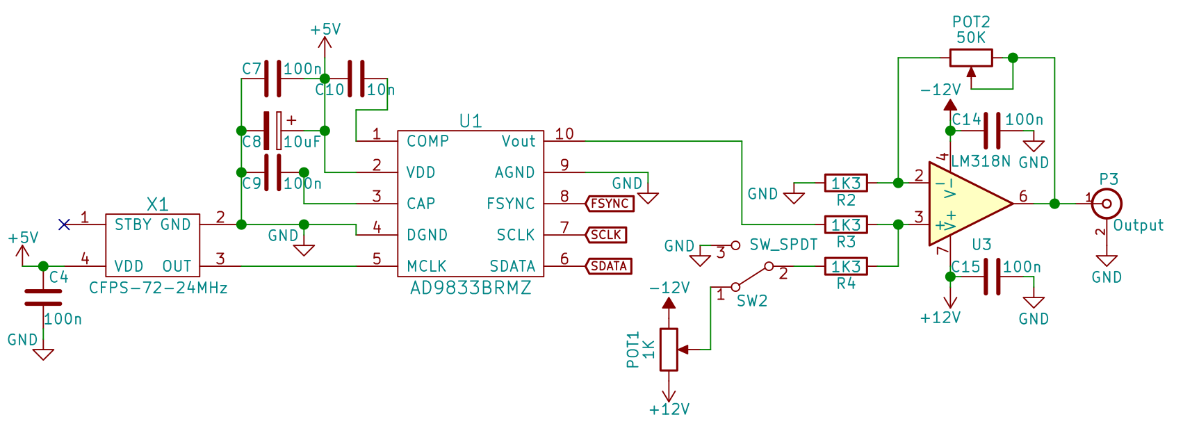
A few paragraphs above when I was talking about the microcontroller connections, I also wrote the Arduino Uno pin equivalents. I did this because the AD9833 circuit described in the previous paragraph is available at various Chinese manufacturers as a breakout board that you can connect to an Arduino Uno. Keep in mind that the output is straight from the IC, without the additional circuitry that I will continue to explain below.
The output of the IC is fed into the non-inverting input of the op-amp using a 1.3kΩ resistor. The trimmer POT1 (a variable resistor), which has its side pins connected to -12V and +12V, has the sweeper connected to a switch's input terminal to provide an offset voltage. The other input terminal of the SPDT switch is wired directly to ground, and the output terminal is connected to the non-inverting input of the op-amp with another 1.3kΩ resistor. This configuration combined with a 50kΩ potentiometer allows us to have a variable gain between 1 and approximately 20. This was computed using Millman’s theorem and the fact that the op-amp keeps its inputs, V+ and V-, at the same voltage:
$$V^{^{+}} = \frac{\frac{V_{in}}{R3} + \frac{V_{offset}}{R4}}{\frac{1}{R3} + \frac{1}{R4}}$$
$$V^{^{-}} = \frac{\frac{V_{out}}{POT2}}{\frac{1}{POT2} + \frac{1}{R2}}$$
$$V^{^{+}} = V^{^{-}}$$
$$V_{out} \approx 20$$
Keep in mind that the gain is also applied to the offset voltage. I did this to have three configurations:
- The offset voltage is set to -350mV using the trimmer POT1. When the switch is in position 3 (R4 connected to ground), the output voltage is the output of the IC, a signal with an amplitude of 350mV and an offset of 350mV, multiplied by the gain set by the potentiometer POT2. When the switch is in position 1 (R4 connected to the offset voltage obtained by the trimmer POT1), the output is just as before minus the offset voltage, essentially a signal with a 350mV amplitude and no offset, multiplied by the gain.
With this configuration, the output voltage can either swing from -7V to +7V or from 0V to what the op-amp is capable of (something near +12V).
- The offset voltage is set to VOUT minimum of the AD9833. This is then multiplied by the gain, which can vary from 1 to 20.
- Instead of the trimmer POT1, you can use a potentiometer and mount it on the front panel so you can have a variable offset. Just remember that the offset is also affected by gain, so it is wise to first set the gain, to choose the peak-to-peak voltage that you need, and after that use the offset potentiometer to adjust the signal's vertical position. I do not recommend this setup; if you want variable offset, I suggest that you add a separate op-amp as a summing amplifier with a fixed gain of 2, as in the schematic below.
$$V_{out} = 40\cdot V_{in} + V_{offset}$$
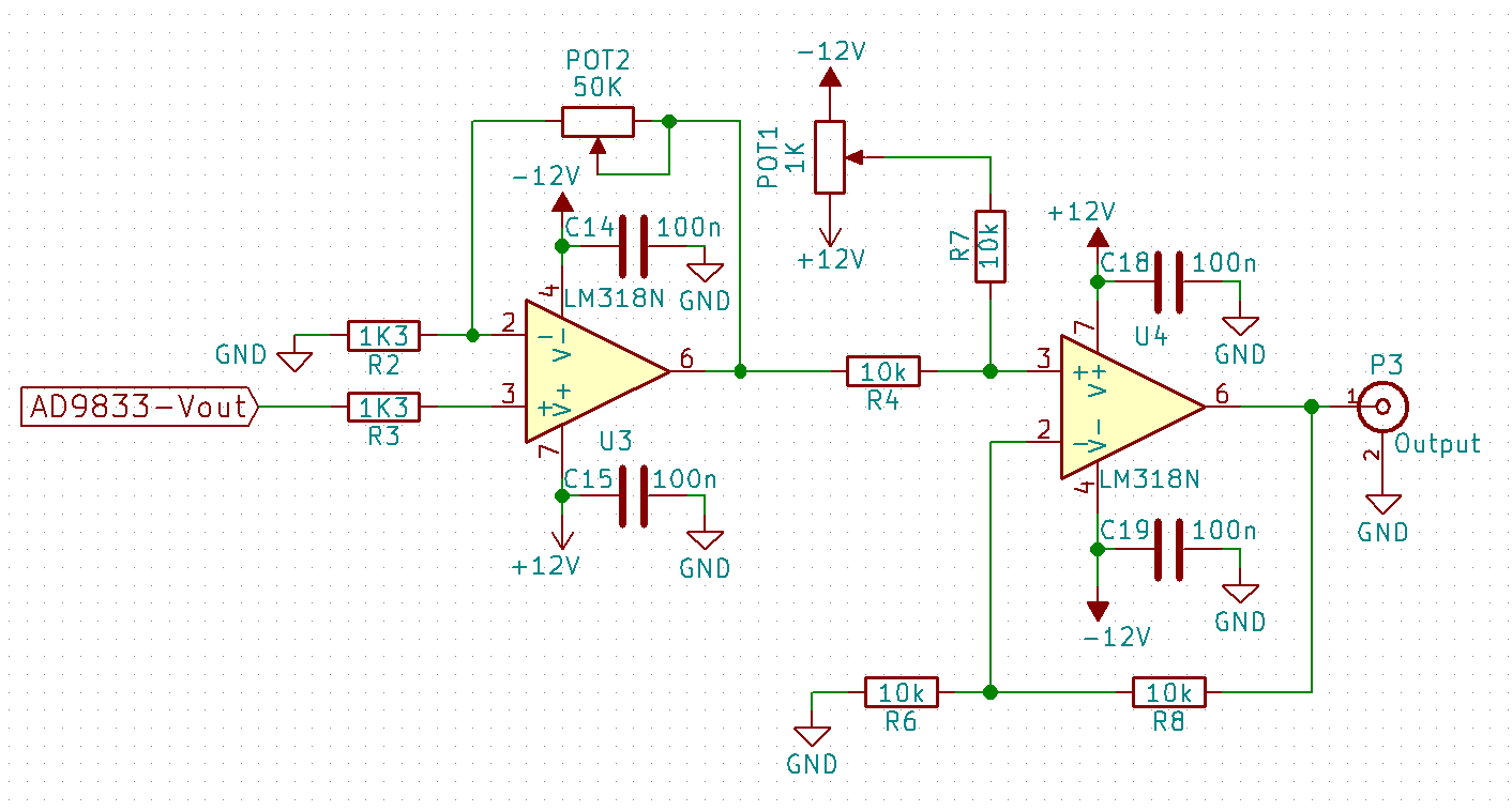
In order to wrap up the amplifying part of the circuit, I have to mention that you will need 100nF decoupling capacitors for both the positive and the negative power supply and that you need to choose an op-amp that can withstand the power supply voltages (+12V and -12V) and that has a very good slew rate, so that it can keep up with high-amplification signals.
Ideally, this circuit should be built on a PCB designed specifically for this application and not on a prototype board. I will provide you with an already designed PCB in KiCad via the files below. However, if you want to make your own, keep these things in mind:
- Place the decoupling capacitor for all of the integrated circuits as close as possible to the power supply pins.
- Try to use a ground plane (if using only two layers, make the bottom layer to consist mostly of ground).
- Separate the analog part of the circuit (the output of the AD9833, the amplifying circuit, and the output BNC connector) from the digital part (microcontroller and communication side of the AD9833). You can split the ground plane right below the AD9833. This can be done easily as the IC has two separate pins for analog and digital ground.
- As the datasheet of the AD9833 suggests, avoid running digital traces under the AD9833.
All the necessary components to build this can be found in the BOM included in the zip file at the bottom of the article.
Now that we are done with building the circuits let’s dive into programming.
Software
To write the code that will be uploaded into the microcontroller’s memory, we will be using the Arduino IDE. In the following few paragraphs I will explain how to write a library for the AD9833 and then the main piece of software that allows us to interface the microcontroller with the AD9833, the LCD, and the rotary encoder. The AD9833 has these so-called registers, which are basically memory locations, into which we can put data, and based on these values the integrated circuit changes its mode of operation; it chooses what waveform to output, the phase, and the division factor. We will be working with five registers: the control register; two phase registers, PHASE0 and PHASE1; and two frequency registers, FREQ0 and FREQ1.
AD9833 Library
We will create two files, AD9833.cpp, the file that will contain the source code, and AD9833.h, its header.
Inside the header, we specify the name of the class (AD9833) and, just like a Russian nesting doll, inside it, variables and functions that we will be calling to communicate with the waveform generator IC and to change its parameters, such as the frequency and the type of waveform. These can be one of two types: public, which we can call from outside the class methods (functions), or private, which we can call only when we are inside a class’s method. I have added comments so that you have an idea about the purpose of every function and variable; for example:
//Initialise the AD9833 //_FYNC is the pin on the uC where FYNC is connected //_mclk is the frequency of the crystal generator AD9833(int _FSYNC, unsigned long _mclk);Going on to the source file, when we initialize a new object of type AD9833 a few things are going to happen; this is inside the function “AD9833::AD9833(int _FSYNC, unsigned long _mclk)”. First, we take note of the FSYNC pin we have passed as an argument, and we set it as an output pin. When writing to the AD9833, this pin will go LOW. Inside this method, we also set some default values for the registers so that we output a sinusoidal signal at 1kHz using the FREQ0 register. The last lines set the SPI to mode2, which is the setting that the microcontroller and AD9833 use to communicate.
All that is remaining now is to carefully read the datasheet and see what values we have to set in the AD9833’s registers to manipulate the output waveform and its operation. Thus, we will write functions for the following operations: write data, set frequency, set phase, sleep, reset, mode, and choose frequency/phase register.
We will be working directly at the bit level. Sometimes we may want to change the value of an entire register, for example for the frequency register, but sometimes we want to only change a few bits of the whole word. To achieve this, we will use the following operations:
- “&=” To set some bits to 0 while leaving the rest undisturbed. (0 = set to 0, 1 = leave it how it is). Example:
controlRegister &= 0xF3FF; // Set D11 and D10 in control register to 0
- “|=” To set some bits to 1 while leaving the rest undisturbed. (1 = set to 1, 0 = leave it how it is). Example:
controlRegister |= 0x0C00; // Set D11 and D10 in control register to 1In the table below I have extracted from the datasheet which bits need to be set to execute the operations.
| Operation | Register | Value |
|---|---|---|
| Set Frequency | FREQ0 | FREEQ0: D15 = 0, D14 = 1 |
| Set Frequency | FREQ1 | FREEQ1: D15 = 1, D14 = 0 |
| Set Phase | PHASE0 | PHASE0: D15 = 1, D14 = 1, D13 = 0 |
| Set Phase | PHASE1 | PHASE0: D15 = 1, D14 = 1, D13 = 1 |
| Set Mode - Sine | CNTRL | D5 = 0, D1 = 0 |
| Set Mode - Triangular | CNTRL | D5 = 0, D1 = 1 |
| Set Mode - Clock | CNTRL | D5 = 1, D1 = 0 |
| Set Frequency Register | CNTRL | D11 = 0 (choose FREQ0); D11 = 1 (choose FREQ1); |
| Reset | CNTRL | D8 = 0 or 1 |
| Sleep - No power-down | CNTRL | D7 = 0, D6 = 0 |
| Sleep - DAC powered down | CNTRL | D7 = 0, D6 = 1 |
| Sleep - Internal clock disabled | CNTRL | D7 = 1, D6 = 0 |
| Sleep - DAC powered down and internal clock disabled | CNTRL | D7 = 1, D6 = 1 |
The registers have different sizes. The control register is 16 bits long, the phase registers are 12 bits long, and the frequency registers have 28 bits. To output data via SPI, we send one byte at a time, as can be seen in the “writeData” function, starting with the low byte (first 8 bits from the data integer) and then the high byte.
Setting the frequency is a bit more tricky because we are not directly sending the frequency that we want. According to the datasheet, the analog output is fMCLK/228 × FREQREG. Thus, the frequency register must be set to:
$$FREQREG = \frac{frequency \cdot 2^{28}}{f_{mclk}}$$
Because the obtained number can be as long as 28 bits, we divide it into two words, each 16 bits long, and then we send the data starting with the lower one.
The rest of the methods should be straightforward if you follow the table above and my indications in the comments.
Main Routine
For the main code that will connect our AD9833, LCD, rotary encoder, and microcontroller together we are going to cheat a bit and use some very well written libraries for the LCD, which uses the I2C bus, and for the rotary encoder.
Our arbitrary waveform generator does not make good use of the phase functionality; I have decided to keep this feature unavailable, but you can use it by uncommenting the directive “//#define usePhase”. However, doing that will disable the ability to choose between the FREQ0 and FREQ1 registers.
I tried to make the software as user-friendly as possible. From the start, on the LCD you can see the frequency in the upper left corner and change it digit by digit, in the upper right corner is the power state of the analog output, which can be either ON or OFF, meaning you can turn off the output without turning off the device. In the bottom left corner, you can choose the register used for storing the frequency, either FREQ0 or FREQ1. This is useful in case you want to easily switch between two different frequencies. Lastly, in the bottom right corner is the type of waveform that you want to output, either sine wave, triangular wave, or rectangular wave. Keep in mind that the clock output will always have a higher amplitude, as the AD9833 outputs it at 2.5V as opposed to 0.65V for sinusoidal and triangular signals.
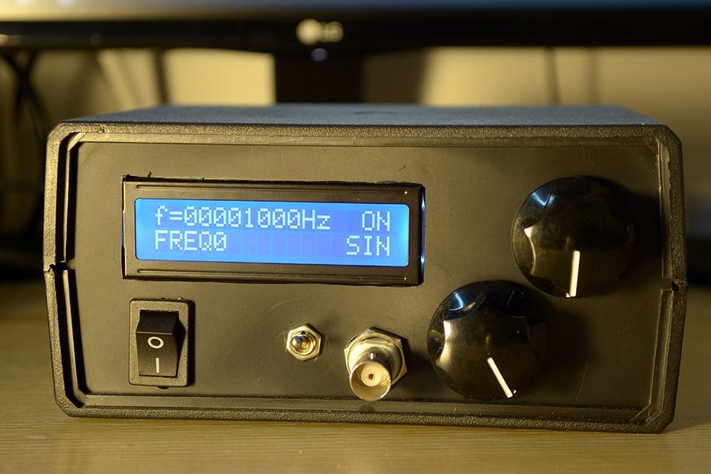
This is how you make changes: Pressing the encoder makes the cursor active, and then you rotate the encoder to "scroll" (move) between the four settings (frequency, ON/OFF, FREQ0/1, and waveform type). After selecting the setting to be changed, pressing the encoder will either change the setting (if ON/OFF or FREQ0/1 has been selected), or you can change the setting's value by rotating the encoder (rotating increments/decrements the current digit or changes the waveform type, depending on the chosen setting). Pressing again applies the setting (for waveform type) or goes to the next digit (for frequency).
I have tried to make the code as concise as possible, and comments are available to help you understand my thought process. If you have any questions, do not hesitate to leave a comment or contact me.
I sincerely hope that everything goes smoothly and you will be able to enjoy your very own Arbitrary Waveform Generator.
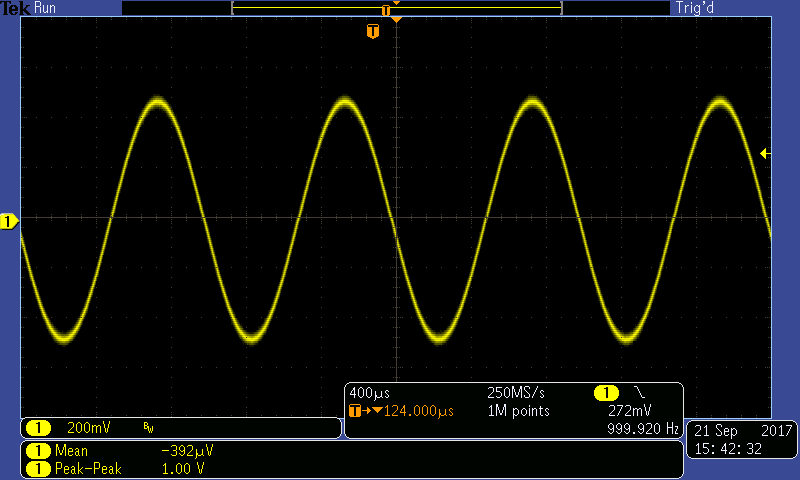
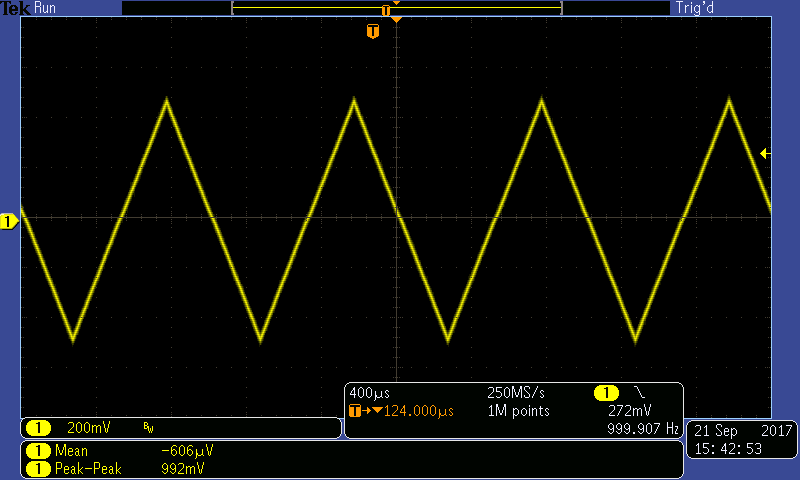
Below are some output waveforms for you to enjoy:
sine wave, 1V peak-to-peak, 1kHz, no offset
triangular wave, 1V peak-to-peak, 1kHz, no offset
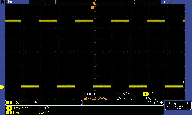
clock signal, 11V peak-to-peak, 500Hz, with offset


What’s the approximate BOM cost for this circuit?