
How to Monitor Current with an Op-Amp, a BJT, and Three Resistors
This article, part of AAC’s Analog Circuit Collection, explains the functionality of a clever circuit that accurately measures supply current.
This article, part of AAC’s Analog Circuit Collection, explains the functionality of a clever circuit that accurately measures supply current.
First of all, I have to admit that the title is slightly misleading. The circuit presented in this article does indeed require only an op-amp, a transistor, and three resistors. It is not, however, a self-contained current monitor in the sense that it measures current and initiates actions based on the measurements. So maybe “current measurer” would be more accurate than “current monitor,” but even “current measurer” doesn’t quite capture it because the circuit doesn’t record the current values or convert them into a visual indication.
In the end, I suppose the circuit is little more than a “current-to-voltage converter,” but keep in mind that it converts current to voltage in a way that is compatible with supply-current-monitoring applications. So maybe we should call it a “current-to-voltage converter for power-supply-current-delivery-monitoring applications” (abbreviated CTVCFPSCDMA). Perfect.
Why?
There are various situations in which you might want to measure the current consumed by your design. Maybe you want to dynamically adjust the functionality of one subsystem based on the current consumption of another subsystem. Maybe you’re trying to estimate battery life, or to establish the smallest-possible regulator IC that can provide adequate output current. You could even use recorded current-consumption measurements as a minimally invasive way of tracking a microcontroller’s transitions between higher- and lower-power states.
How?
As discussed in the opening paragraphs, this circuit converts current to voltage. This might fulfill your current-monitoring requirements if all you need to do is manually observe current-consumption behavior using a multimeter or an oscilloscope. I suppose you could even record and analyze your current-consumption measurements using a data-acquisition device and some appropriate software.
If you need a circuit that is more autonomous in its ability to record and/or respond to current consumption behavior, you’ll probably want to digitize the measurements using a microcontroller. If only basic functionality is required and you have no other need for a processor, you could use a comparator or an analog window detector.
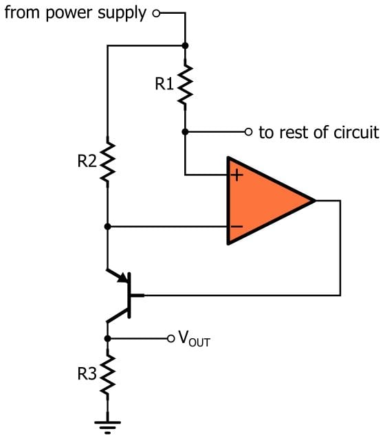
The Circuit
The CTVC... presented in this article is based on a circuit found in an application note entitled “Op Amp Circuit Collection,” published (back in 2002) by National Semiconductor. My version looks like this:
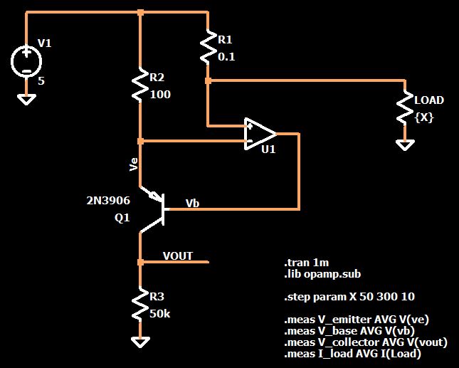
And here is my LTspice implementation:
This may look a bit confusing at first glance, but the operation really is rather straightforward. Let’s walk though it:
- The current flows from the power supply, through R1, to the load. R1 functions as a typical current-sensor resistor, and like other current-sense resistors it has a very low resistance so as to reduce power dissipation and minimize its effect on the measurements and on the load circuit.
- The voltage applied to the op-amp’s non-inverting input terminal is equal to the supply voltage minus (supply current × R1).
- Don’t let the PNP transistor distract you from the fact that the op-amp does indeed have a negative feedback loop. The presence of negative feedback means that we can apply the virtual short approximation, i.e., we can assume that the voltage at the inverting input terminal is equal to the supply voltage minus (supply current × R1).
- Since the upper terminal of both R1 and R2 is tied to the supply voltage, the virtual-short assumption tells us that an equal voltage appears across both of these resistors, and consequently the current through R2 is equal to the current through R1 divided by the ratio of R2 to R1. In the LTspice circuit shown above, R2 is 1000 times larger than R1, which means that the current through R2 will be 1000 times smaller than the current through R1.
- The BJT’s base current is very small, so we can say that the current through R3 is more or less equal to the current through R2. Thus, we use R3 to create a voltage that is directly proportional to the current through R2, which in turn is directly proportional to the current through R1.
Here’s a diagram that should help to clarify and reinforce this explanation:
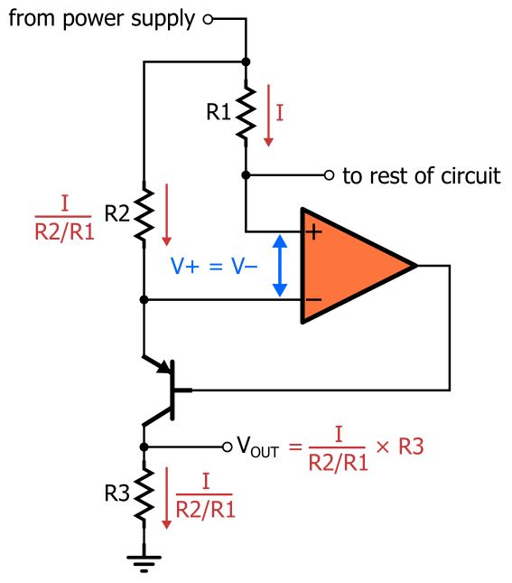
As you can see, the final equation for VOUT is
$$V_{OUT}=\frac{I_{LOAD}}{R2/R1}\times R3 = \frac{R1\cdot R3}{R2}\times I_{LOAD}$$
What Exactly Is That PNP Doing...?
You can think of the transistor in two ways: as an adjustable valve that allows the op-amp to increase or decrease the current flowing through R2 and R3, or as a variable voltage-dropping device that the op-amp can use to establish the correct voltage at the VOUT node. In both cases the end result is the same: the transistor is the means by which the op-amp can force the voltage at the inverting input terminal to equal the voltage at the non-inverting input terminal.
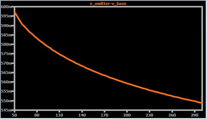
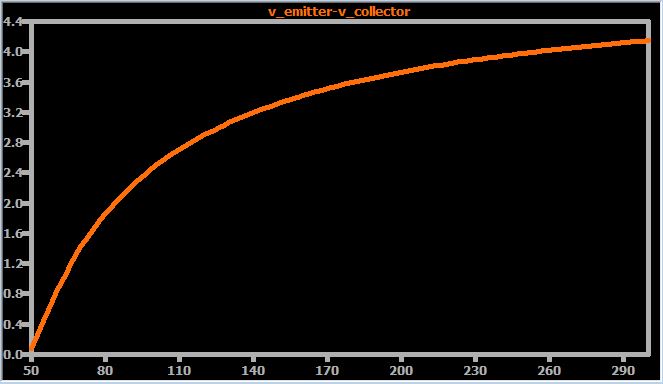
The transistor really is the most interesting part of this circuit. We often use BJTs in “on or off” applications, and it’s important to recognize that the situation in this circuit is completely different. The op-amp (with the help of negative feedback, of course) is actually making small, precise adjustments to the PNP’s emitter-to-base voltage (VEB). The following plot shows VEB for a range of load currents (corresponding to load resistances from 50 Ω to 300 Ω).
For information on how to create a plot with a stepped parameter on the horizontal axis, see this page.
Notice how all of these voltages are near the typical turn-on threshold (~0.6 V) for a silicon pn junction. What this tells you is that the op-amp is very carefully negotiating the BJT’s threshold region in order to produce the required—and relatively large—changes in the emitter-to-collector voltage drop. The entire range of VEB values is only ~50 mV, and compare this ~50 mV variation to the ~4 V variation in emitter-to-collector voltage:
Performance
Real implementations of this circuit will, of course, have error sources that cause the load current vs. output voltage relationship to deviate from the ideal formula given above. Even the LTspice circuit isn’t quite perfect because of the realistic behavior incorporated into the BJT model (and perhaps the op-amp model as well). However, if you have high-precision resistors and a good op-amp, I think that this circuit can be quite accurate. The following plot conveys the simulated error over the same load-resistance range (keep in mind that “V_collector” is the same as VOUT).
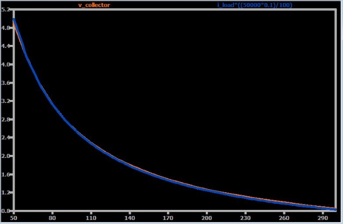
The two traces almost perfectly overlap, indicating good accuracy. Notice how the orange trace is noticeably lower than the blue trace at the smallest resistance value; this occurs because a load resistance of 50 Ω corresponds to an output voltage of 5 V, but VOUT cannot be exactly 5 V because at least a little bit of voltage must be dropped across R2 and across the emitter-collector junction.
Conclusion
We’ve covered an interesting and effective circuit that accurately converts supply current into a voltage that can be measured, digitized, or used as an input to a comparator. If you would like to continue exploring this handy circuit, feel free to save yourself a bit of work by downloading my LTspice schematic (just click on the orange button).


NIce !!!
This explanation is excellent. It is very helpful in understanding these circuits. However, I still don’t fully understand the design philosophy behind this circuit with regard to the BJT. In particular, when analyzing a circuit, I have a problem identifying what the “absolutes” are. For example, the op amp wants to maintain the same voltage at the inverting and non-inverting inputs. The EB junction of the BJT is somewhat fixed at approximately 0.6v. The section, “What Exactly Is That PNP Doing…” was exactly what I wanted to see in that part of the article, but I’m still missing some nuance in the use of the BJT.