
Thermocouple Signal Conditioners and Signal Conditioning Near the Cold Junction
Learn about monolithic thermocouple signal conditioners and signal conditionings through example products like AD594 / AD595, MAX6675, and ADS1220.
Previously in this series, we looked at the principles of operating monolithic thermocouple signal conditioners. Furthering our discussion, this article explores a few other options for thermocouple applications, namely the AD594/AD595, the MAX6675, and the ADS1220. Some of the previous article's basic concepts also apply to the thermocouple conditioners discussed here. For example, all of these signal conditioners should be placed near the cold junction of the thermocouple. However, some features might be device-specific.
To stay concise, we’ll try to focus mainly on the key features of each of these devices.
Thermocouple Signal Conditioner Example 1—AD594/AD595
The AD594/AD595 is a complete thermocouple signal conditioner that integrates an amplifier and cold junction compensator into a single package. Figure 1 shows the functional block diagram and the basic single-supply connection of the device.
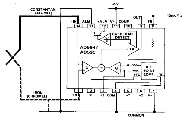
Figure 1. AD594/AD595 block diagram. Image used courtesy of Analog Devices
A fundamental portion of the circuit is the feedback loop created by the right-hand differential amplifier (with gain G), the main amplifier (+A), and the internal resistor between pins 8 and 5. The left-hand differential pair amplifies the thermocouple voltage and applies it to a summing node in the feedback loop. The “Ice Point Comp” block produces the cold junction compensation (CJC) voltage and adds it into the thermocouple loop through the right-hand differential pair.
You can find details about how this circuit works in the AD594/AD595 datasheet. Without going further into these details, the end result is that the device is designed to directly connect to the thermocouple, perform cold junction compensation and amplification, and produce a 10 mV/°C output. For example, with a type J thermocouple connected to the AD594, the output will be about 500 mV when the hot junction is at 50 °C.
Note that the AD594 and AD595 are pre-calibrated by laser wafer trimming to match the characteristic curves of type J and K thermocouples, respectively.
Measuring Negative Temperatures in the AD594/AD595
In a previous article, we discussed that the AD849x, which is also a thermocouple signal conditioner, can measure negative temperatures even when powered by a single-rail supply. Unlike the AD849x, the AD594/AD595 needs a dual-rail supply to measure temperatures below 0 °C.
AD594/AD595 Gain Calibration
One interesting feature of the AD594/AD595 is that certain important nodes of the internal circuitry are available at the package pins. For example, pin 8 is connected to the internal feedback path of the device. Also, the CJC voltage, which is applied to the right-hand differential amplifier, is available at pins 3 and 5. Making these nodes available at the package pins allows us to have a more flexible signal conditioner that can be adjusted depending on the application requirements.
With that in mind, let’s see how access to the feedback resistor can be used in practice. As shown in Figure 1, under normal operation conditions, pins 9 and 8 are tied together. This connects the amplifier output to the internal feedback resistor that sets the device gain. The internal feedback network is factory-calibrated to produce a 10 mV/°C output. However, to adjust the gain, we can place an additional resistor between pins 9 and 5. This external resistor will be in parallel with the internal feedback resistor, enabling adjustments to the amplifier gain. We can even replace the internal resistor with the external one by removing the connection between pins 9 and 8.
Figure 2 illustrates gain calibration by adjusting the feedback resistor.
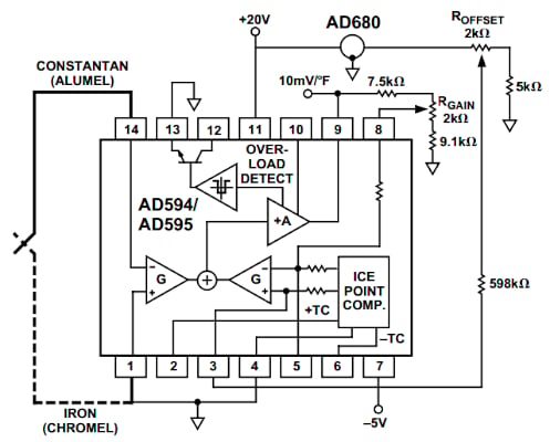
Figure 2. Diagram showing the gain calibration by adjusting the feedback resistor. Image used courtesy of Analog Devices
The above diagram shows how the AD594/AD595 can be used to produce an output proportional to the temperature on a Fahrenheit scale (10 mV/°F). Next, let's consider the following equation for the temperature scale conversion:
\[Degrees\,Fahrenheit=\frac{9}{5}(Degrees \,Celsius)+32\]
From that equation, we can verify that we need to increase the gain by \(\frac{9}{5}\) (as well as add an appropriate offset value) to have an output that changes at 10 mV/°F rather than the factory-calibrated value of 10 mV/°C.
In other words, we need to adjust the feedback resistor to have a \(10\times\frac{9}{5}=18 mV/°C\) output.
The above diagram achieves this by placing a trimming potentiometer between pins 9 and 8. For a type J thermocouple, the room temperature sensitivity is 51.7 μV/°C. Therefore, the resulting gain for the AD594 can be found as:
\[Gain_{New}=\frac{18 mV/°C}{51.7 μV/°C}=348.16\]
As explained in this application note, we can apply an AC signal, VTest, to pins 1 and 14 and then adjust RGain until we get VTest ⨉ GainNew at the output.
AD594/AD595 Offset Calibration
It is also possible to add an offset to the output of the AD594/AD595. One way to perform offset calibration is shown in Figure 3.
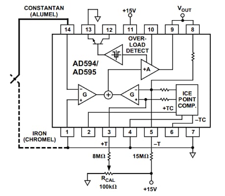
Figure 3. Diagram showing one way to perform offset calibration. Image used courtesy of Analog Devices
This can be particularly helpful when trimming out the residual calibration error of the device. The AD594/AD595 is a laser wafer trimmed to achieve a maximum calibration error of 1°C or 3°C, depending on the device performance grade. With a demanding application, one can use the above diagram to trim out this residual error. The 15 MΩ resistor slightly increases the potential of the inverting input of the right-hand differential amplifier. This forces the circuit to have a negative offset of about -3 °C. The “forced” negative offset is then calibrated out through the resistive network connected to the non-inverting input of the differential amplifier. This calibration scheme insures that a single uni-directional trim can be used to null the error. You can see another example of offset calibration in Figure 2.
Temperature Adjustments for Other Thermocouple Types
In addition to tweaking the gain and offset, it is possible to adjust the temperature coefficient of the internal cold junction compensator. This allows us to use the AD594/AD595 with other types of thermocouples. For example, the datasheet explains how the AD594, which is factory-calibrated for type J thermocouples, can be recalibrated to condition E-type thermocouples.
Thermocouple Signal Conditioner Example 2—MAX6675
Another option for thermocouple signal conditioning is the MAX6675, whose functional block diagram is shown below.
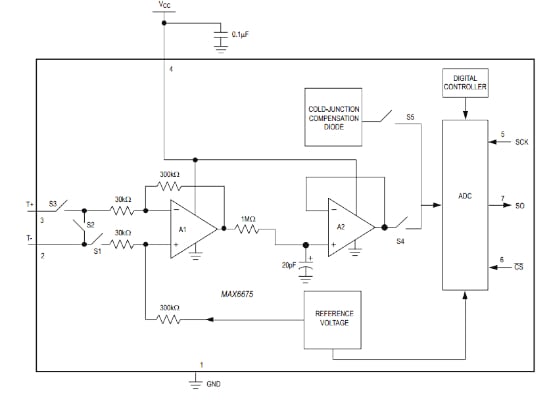
Figure 4. Block diagram for MAX6675. Image used courtesy of Maxim Integrated (Analog Devices)
The MAX6675 integrates a 12-bit ADC (analog to digital converter) and cold junction compensator into a single package. It can directly connect to a type K thermocouple, as shown in Figure 5.
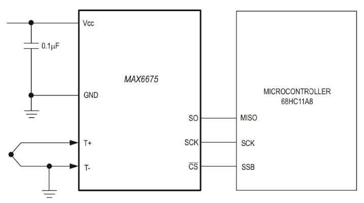
Figure 5. Example application circuit diagram. Image used courtesy of Maxim Integrated (Analog Devices)
The device can measure a wide range of hot-junction temperatures from 0 °C to 1024 °C (note that it cannot measure negative temperatures). The cold junction temperature or the operating temperature of the MAX6675 should be in the range from -20 °C to +85 °C.
As shown in Figure 4, both the CJC signal and the thermocouple output are digitized by the ADC. The device uses this information to perform CJC and reads out the result (i.e. the temperature is measured as a 12-bit value onto the SO pin). A sequence of all zeros corresponds to 0 °C, whereas a sequence of all ones means the thermocouple is at +1023.75 °C.
Thermocouple Signal Conditioner Example 3—ADS1220
As the third thermocouple conditioner option, I’d like to mention that rather than using a device with an integrated cold junction compensator, you can also use an ADC that includes an internal precision temperature sensor. An example diagram that uses the ADS1220 is shown in Figure 6.
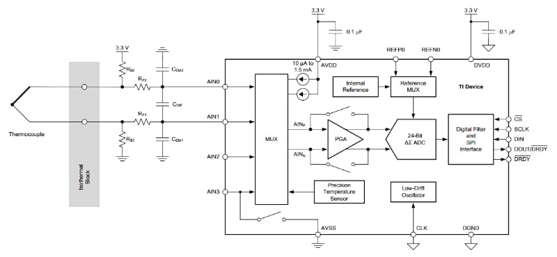
Figure 6. Block diagram for ADS1220. Image used courtesy of Texas Instruments
The ADS1220 is a 24-bit ADC with a high-precision temperature sensor that can be used to measure the device temperature for CJC purposes. The ADS1220 cannot automatically perform cold junction compensation; however, it can be done in the processor that follows the ADC. If using the internal temperature sensor is not possible, for example, because of its limited accuracy or because we cannot place the ADC near the cold junction, we can use an RTD or a thermistor to measure the cold junction temperature. This will, however, consume an additional input channel from the ADC.
To see a complete list of my articles, please visit this page.


