
AXI Interconnects Tutorial: Multiple AXI Masters and Slaves in Digital Logic
This article will explore AXI interconnects, the digital logic that allows multiple AXI masters and AXI slaves to communicate.
In the last article, we introduced AXI, the Advanced Extensible Interface, part of the ARM AMBA specification for SoC design.
AXI uses well defined master and slave interfaces that communicate via five different channels:
- Read address
- Read data
- Write address
- Write data
- Write response
Figure 1 shows the five AXI channels.
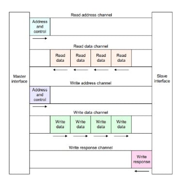
Figure 1. AXI Channels
For connecting a single master to a single slave those five channels are all that is needed. For connecting multiple masters and/or multiple slaves a different approach is required.
Enter the AXI Interconnect.
AXI Transactions
An AXI Interconnect manages the AXI transactions between AXI masters and AXI slaves.
In the previous AXI article, a number of AXI signals were associated with each of the five channels. To understand how an interconnect handles these signals, a closer look at a simple AXI transaction is needed.
Read Transactions
Figure 2 shows a timing diagram of a read transaction between an AXI master and slave.
Note that some of the signals have been omitted for clarity. The burnt orange represents a master controlled signal, while the blue is a slave controlled signal.
To start the transaction off, the master places the slave's address on the ARADDR line and asserts that there is a valid address (ARVALID). Following time T1, the slave asserts the ready signal (ARREADY). Remember the source of data asserts the valid signal when information is available, while the receiver asserts the ready signal when it is able to consume that information. For a transfer to occur both READY and VALID must be asserted. All of this happens on the read address channel, with the address transfer completing on the rising edge of time T2.

Figure 2. AXI Read Transaction
From here, the rest of the transaction occurs on the read data channel. When the master is ready for data it asserts its RREADY signal. The slave then places data on the RDATA line and asserts that there is valid data (RVALID). In this case, the slave is the source and the master is the receiver.
Recall that VALID and READY can be asserted in any order so long as VALID does not depend on READY. This read represents a single burst transaction made up of 4 beats or data transfers. Notice the slave asserts RLAST when the final beat is transferred.
Write Transactions
What about writes? Figure 3 shows a timing diagram of an AXI write transaction. The addressing phase is similar to a read. A master places an address on the AWADDR line and asserts a valid signal. The slave asserts that it's ready to receive the address and the address is transferred.
Next, on the Write Data Channel, the master places data on the bus and asserts the valid signal (WVALID). When the slave is ready, it asserts WREADY and data transfer begins. This transfer is again 4 beats for a single burst.
The master asserts the WLAST when the last beat of data has been transferred. In contrast to reads, writes include a Write Response Channel where the slave can assert that the write transaction has completed successfully.

Figure 3. AXI Write Transaction
The AXI Interconnect
Recall that in AMBA Revision 2.0, connecting multiple AHB masters to an AHB slave required an AHB Arbiter that granted permission to the master with higher priority.
In order to connect a single AHB master to multiple AHB slaves, an AHB decoder that inspected an input address and connected the appropriate slave was used. Figure 4 shows an example of these two scenarios.

Figure 4. AHB Arbiter and AHB Decoder for multi-master/multi-slave system
This is where AXI provides the most flexibility. Instead of prescribing how multi-master and multi-slave systems work, the AXI standard only defines the interfaces and leaves the rest up to the designer. If the system has multiple masters attempting to communicate with a single slave, then the AXI Interconnect may contain an arbiter that routes data between the master and slave interfaces. This arbiter could be implemented using simple priorities, a round-robin architecture, or whatever suits the designer's needs.
Figure 5 shows an interconnect connecting multiple masters to a slave device.

Figure 5. AXI Interconnect with multiple masters
What about if there are multiple slaves with a single master? For this to work the interconnect would need to interpret the address and route the transaction to the proper slave. In this case a decoder could work.
Figure 6 shows a single master communicating to multiple slaves via a decoder contained within the interconnect logic.

Figure 6. AXI interconnect with multiple slaves
Systems that use multiple masters and multiple slaves could have interconnects containing arbiters, decoders, multiplexers, and whatever else is needed to successfully process transactions. This might include logic to translate between AXI3, AXI4, and AXI4-Lite protocols.
Additionally, interconnects can perform bus-width conversion, use data FIFOs, contain register slices to break timing paths, and even convert between two different clock domains.
Figure 7 shows an interconnect with multiple masters and slaves.
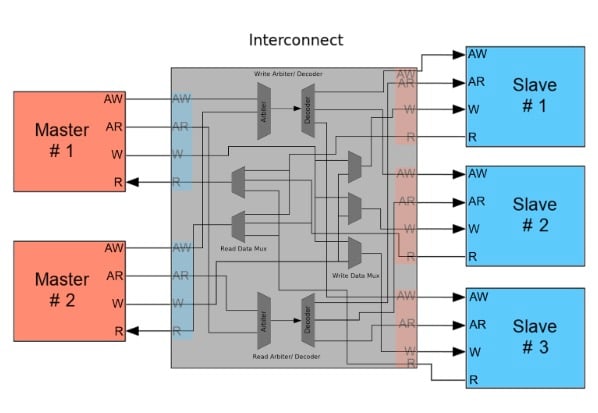
Figure 7. AXI Interconnect Multi-Master/Multi-Slave
Here the write address channel and the read address channel have their own dedicated arbiters and decoders; this way reads and writes can happen simultaneously. To see how this works, an example is necessary. In one scenario, a master would put an address on the write address (AW) channel and the arbiter would grant it permission and pass the address to the decoder. The decoder would then select the correct slave to write the address to.
Next, the write data mux would open a path to the same slave so that the master and slave could use the write data channel (shown as W) to perform transfers. Meanwhile, the other master could be reading data from the same or a different slave using the read (R) and read address (AR) channel, with the read mux opening a path between the two. Keep in mind, Figure 7 is just one example of how an interconnect might be laid out.
Notice the master and slave interfaces built into the interconnect. As mentioned earlier, the AXI standard only defines the interfaces. Thus, the only way to connect an AXI master to an interconnect is via an AXI slave interface. The same rule applies when connecting a slave to the interconnect, i.e., it must be connected to an AXI master interface.
Interconnects in Design
Depending on the system's requirements, designing a custom AXI Interconnect may not be the best decision. Vendors like Xilinx provide AXI Interconnects for use with both their IP and any IP that conforms to the AMBA standard. Altera (now Intel), another vendor, provides interconnects that map Avalon transactions to AXI devices.
There are also a number of open source designs. For example, some of the projects on opencores.org include AXI master and slave interfaces as well as a generic interconnect design. There are even smart interconnects that detect how many masters and slaves they are connected to and automatically implement the logic needed to control them.
Figure 8 shows two interconnect implementations. Figure 8a is the Qsys Interconnect from Altera, which allows Avalon, AXI, and APB transactions to move between master and slave. Figure 8b shows the Xilinx generic AXI Interconnect for use with AXI3, AXI4, and AXI4-Lite components.

Figure 8. Altera/Intel (a) and Xilinx (b) both offer interconnects
While implementing a custom interconnect can be difficult and time-consuming, when something doesn't work right investigation can prove much easier because the HDL code is open and available.
Vendor-provided interconnects are essentially black boxes. If one of them has a bug, it could be very hard to locate or correct the issue. That being said, many of the vendor interconnects have been vetted over time and are usually safe to use.
Conclusion
This article introduced the AXI interconnect, a digital logic block that allows multiple AXI masters to communicate with multiple AXI slaves. AMBA Revision 3.0 specifically left the details of interconnects undefined to keep the AXI protocol flexible and extensible.
An interconnect can contain a number of different digital components depending on what's connected to them. This could be arbiters, decoders, and multiplexers or protocol converters, register slices, and clock converters.
The AXI Interconnect is a fundamental component in any AXI system and represents the glue between masters and slaves. Having intuition on how an interconnect works makes building and troubleshooting any AXI system a whole lot easier.


Very good article, I would like to ask which open source Interconnect in open Cores.org you mentioned in the article is, I would like to use it as a reference, thank you