Microstrip Impedance Calculator
This calculator helps you compute the characteristic impedance of a microstrip.
Output
Overview
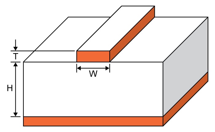
This calculator is designed to calculate the characteristic impedance of a microstrip - a flat conductor suspended over a ground plane with a dielectric between them (see diagram below). While commonly constructed using printed circuit boards, this structure can also be built using other materials as long as there is a conductor separated from a ground plane by some dielectric material.
Just enter the given values for trace thickness, substrate heights, trace width and substrate dielectric in the calculator above and press the "calculate" button. The default units for all given values, except the substrate dielectric, is in mil. It is possible to select other units.
Equations
$$Z_{0}=\frac{\eta _{0}}{2\pi \sqrt{2}\sqrt{E_{r}+1}}ln\left ( 1+4\left ( \frac{H}{W_{eff}} \right ) (X_{1}+X_{2})\right )$$
Where:
$$W_{eff}=W+\left ( \frac{t}{\pi } \right )ln\left \{ \frac{4e}{\sqrt{(\frac{T}{H})^2+(\frac{T}{W \pi+1.1T\pi})^2}} \right \}\frac{E_{r}+1}{2E_{r}}$$
$$X_{1}=4(\frac{14E_{r}+8}{11E_{r}})(\frac{H}{W_{eff}})$$
$$X_{2}=\sqrt{16(\frac{H}{W_{eff}})^2(\frac{14E_{r}+8}{11E_{r}})^2+(\frac{E_{r}+1}{2E_{r}})\pi^2}$$
$$Z_{0}$$ = characteristic impedance of the microstrip in ohms (Ω).
$$H$$ = subtrate height
$$W$$ = trace width
$$T$$ = trace thickness
$$\epsilon_{r}$$ = substrate dielectric
Applications
Microwave antennas and couplers, as well as some filters, can be created using the microstrip. Since they are just patterns of metallization on a substrate, the microstrip device is far cheaper than the traditional waveguide, as well as being more compact and lighter. However, microstrips cannot handle power levels as high as waveguides can. Microstrips also have issues in power loss, cross-talk and unintentional radiation because they are not enclosed like the waveguide.
Aside from microwave applications, microstrips also find themselves in high-speed digital PCB design. Such application entail signal travel with minimal distortion and no cross-talk and/or radiation - areas where the microstrip excel as long as not handling very high frequencies.