 Facebook
 Google
 GitHub
 Linkedin
Practical PCB Layout Tips Every Designer Needs to Know
This article contains practical PCB layout tips that can help your PCB projects work correctly and reliably.
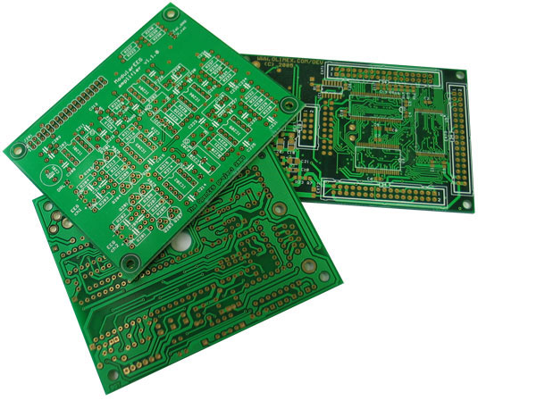
Practical PCB Layout Tips
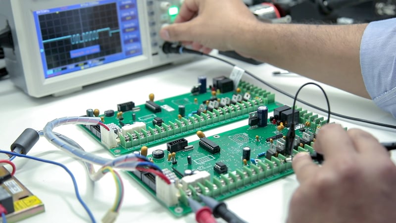
Engineers tend to pay most attention to circuits, the latest components, and code as important parts of an electronics project, but sometimes a critical component of electronics, the PCB layout, is neglected. Poor PCB layout can cause function and reliability problems. This article contains practical PCB layout tips that can help your PCB projects work correctly and reliably.
Sizing Traces
Real-world copper traces have resistance. This means that a trace has a voltage drop, power dissipation, and a temperature rise when current flows through it. Resistance is defined by this formula:
$$R=\frac{(resistivity*length)}{(thickness*width)}$$
PCB designers most commonly use length, thickness, and width to control the resistance of a PCB trace. Resistance is a physical property of the metal used to make the trace. PCB designers can't really change the physical properties of copper, so focus on the trace size, which you can control.
PCB trace thickness is measured in ounces of copper. One ounce of copper is the thickness we would measure if we evenly spread 1 oz of copper over a 1 square foot area. This thickness is 1.4 thousandths of an inch. Many PCB designers use 1 oz or 2 oz copper, but many PCB manufacturers can provide 6 oz thickness. Note that fine features like pins that are close together are hard to make in thick copper. Consult your PCB manufacturer about what their capabilities are.
Use a PCB trace width calculator to determine how thick and wide your traces should be for your application. Aim for a 5°C temperature rise. If you have extra space on the board, use bigger traces, as they don’t cost anything.
When doing a multi-layer board, remember that traces on external layers have better cooling than traces on internal layers because the heat from inner layers has to travel through layers of copper and PCB material before being conducted, radiated, or connected away.
Make Loops Small
Loops, especially high frequency loops, should be made as small as possible. Small loops have lower inductance and resistance. Placing loops over a ground plane further reduces inductance. Having small loops reduces high frequency voltage spikes caused by $$V=L\frac{di}{dt}$$. Small loops also help reduce the amount of signals that are inductively coupled into the node from external sources, or are broadcast from the node. This is what you want, unless you’re designing an antenna. Also keep loops small for op-amp circuits to prevent noise from being coupled into the circuit.

Decoupling Capacitor Placement
Place decoupling capacitors as near as possible to the power and ground pins of integrated circuits to maximize decoupling efficiency. Placing capacitors farther away introduces stray inductance. Multiple vias from the capacitor's pin to a ground plane reduce inductance.

Kelvin Connections
Kelvin connections are useful for measurements. Kelvin connections are made at the exact points to reduce stray resistance and inductance. For example, Kelvin connections for a current sense resistor are placed exactly at the resistor pads, not at some arbitrary place on the traces. Although on the schematic, placing the connections at the resistor pads or at some arbitrary point may look the same, real traces have inductance and resistance that could throw your measurements off if you don’t use Kelvin connections.

Keep Digital and Noisy Traces Away from Analog Traces
Parallel traces or conductors form a capacitor. Placing traces close together capacitively couples the signals on the traces, especially if the signals are high frequency. Keep high frequency and noisy traces away from traces that you don’t want noise on.
Ground is Not Ground
Ground is not an ideal conductor. Take care to route noisy grounds away from signals that need to be quiet. Make ground traces large enough to carry the currents that will flow. Placing a ground plane directly under signal traces lowers the impedance of the traces, which is ideal.

Via Size and Number
Vias have inductance and resistance. If you’re routing a trace from one side of the PCB to the other and need low inductance or resistance, use multiple vias. Large vias have lower resistance. This is especially useful in grounding filter capacitors and high current nodes. Use a via size calculator like this one.
Using PCB as Heatsink
Place extra copper around surface mount component to provide extra surface area to dissipate heat more efficiently. Some component datasheets(especially power diodes and power MOSFETs or voltage regulators) have guidelines for using PCB surface area as heatsinks.

Thermal Vias
Vias can be used to move heat from one side of a PCB to the other. This is especially useful when a PCB is mounted on a heatsink on a chassis that can further dissipate heat. Large vias transfer heat more efficiently than small vias. Many vias transfer heat more efficiently than one via, and lower the operating temperature of components. Lower operating temperatures contribute to higher reliability.

Thermal Relief
Thermal relief is making connections between a trace or a fill and a component pin small to make soldering easier. This small connection is short to reduce the impact on electrical resistance. If thermal relief on component pins is not used, then the component may be a little cooler because there’s a better thermal connection to traces or fills that can dissipate heat, but it’ll be harder to solder and desolder.
Distance between Traces and Mounting Holes
Leave room between copper traces or fills and mounting holes; this helps prevent shock hazards. Solder mask isn’t considered a reliable insulator, so take care that there is distance between copper and any mounting hardware.

Heat Sensitive Components
Keep components that are sensitive to heat away from other components that generate heat. Examples of components that are sensitive to heat include thermocouples and electrolytic capacitors. Placing thermocouples close to heat sources may throw off temperature measurements. Placing electrolytic capacitors close to heat generating components will reduce their operating life. Components that generate heat may include bridge rectifiers, diodes, MOSFETs, inductors, and resistors. The heat depends on current flowing through the components.
Conclusion
This article has covered some basic practical PCB layout tips that can positively impact the functionality and reliability of your design. Have more tips and tricks? Leave them in the comments!


Are there PCB designers who can take my hand drawn schematic? They would need to draw the schematic for schematic capture, and then lay out the 4 layer PCB. Then supply me the drawn schematic and the PCB files.