Facebook
 Google
 GitHub
 Linkedin
Embedded PID Temperature Control, Part 2: Board-Level Integration
This article covers the firmware that allows the EFM8 microcontroller to communicate with the DAC and the MAX31855.
This article covers the firmware that allows the EFM8 microcontroller to communicate with the DAC and the MAX31855.
Supporting Information
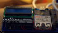
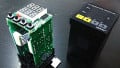
- This project makes use of a custom-designed PCB; please refer to Custom PCB Design with an EFM8 Microcontroller for guidance on incorporating EFM8 devices into your custom hardware.
- You can find a brief overview of thermocouples along with some general information about the MAX31855 in Make an EFM8-Based System for Monitoring and Analyzing Thermocouple Measurements.
- An Introduction to Control Systems: Designing a PID Controller Using MATLAB’s SISO Tool
- Negative Feedback, Part 1: General Structure and Essential Concepts
Previous Article in This Series
From Diagram to Hardware
The previous article presented the following diagram of a PID control system:

From this diagram we can establish three fundamental components of a PID system: the controller, which performs the PID calculations; the plant, which translates the controller’s calculations into physical changes; and the feedback mechanism, which translates the physical changes back into analog or digital signals that can be used in the controller’s calculations. In our PID thermostat, these three components correspond, respectively, to the EFM8 microcontroller, the DAC in conjunction with high-current-drive circuitry (discussed in the previous article), and the MAX31855 thermocouple-to-digital converter. Thus, the success of our project depends upon reliable communication that can integrate these three functional blocks into a unified PID system.
SPI (Simple, Proven Interface)
Actually, SPI stands for Serial Peripheral Interface, but my alternative is certainly appropriate. I value SPI as a straightforward, flexible, low-overhead communications protocol that just might be supported by every microcontroller and DSP on the market. How fortunate, then, that both the MAX31855 and the DAC speak SPI. However, SPI is not a fixed, precisely defined protocol; it is more like a general approach to serial communication. The standard features are as follows:
- Each device on the bus is either a master or a slave. (It is possible to have more than one master, but I recommend avoiding this whenever possible. I2C is a better choice for multi-master systems.)
- The electrical connections consist of a serial-clock signal (SCK), a master-to-slave data signal (MOSI, i.e., master-out-slave-in), a slave-to-master data signal (MISO, i.e., master-in-slave-out), and one slave-select signal (NSS) for each slave device.
- The master initiates all transactions by activating one or more NSS lines and driving clock pulses on SCK. The transaction continues as long as NSS is active.
- A transaction can involve data transfer from master to slave (via MOSI), from slave to master (via MISO), or both. The master can send data to multiple slaves by activating all their NSS lines, but to avoid driver contention the slaves must incorporate some method of sharing the MISO signal.
The following schematic shows the hardware design for the devices on the SPI bus.

Impeccable Timing
These two diagrams convey the details of the SPI timing for the two slaves on our bus. The first is from the MAX31855’s datasheet, and the second is from the DAC’s datasheet.


In the diagram for the MAX31855, CS is used instead of NSS. CS stands for “chip select,” and the overline indicates that its active state is logic low; NSS stands for “not slave select,” where “not” (instead of an overline) indicates that it is an active-low signal.
In the diagram for the DAC, SYNC with an overline is used instead of NSS, though in this case the situation is a little more complicated. The DAC is designed to be compatible with a variety of serial communication protocols; this is why the timing diagram doesn’t look like typical SPI. But typical SPI works fine, and that is what we’re going to use.
If you look closely at these two diagrams, you’ll notice a small but crucial discrepancy: With the MAX31855, the first clock transition after the NSS falling edge is a low-to-high transition. With the DAC, it is a high-to-low transition:

This means that we need to adjust the EFM8’s SPI configuration according to which slave we are talking to. The following diagram illustrates the four clock configuration options offered by the EFM8’s SPI peripheral; simply compare the device’s timing details to this diagram to determine the proper configuration.

Arranging Data
SPI is a malleable protocol, and this applies not only to timing details but also to data formatting. The MAX31855 transmits data as one 32-bit word, as follows:

We are not going to worry about error handling for this project, and we don’t need to know the MAX31855’s internal temperature, so all the information we need is contained in the first 14 bits (bit 31 to bit 18). However, the EFM8’s SPI peripheral operates in units of bytes, so we will read two bytes from the MAX31855 then ignore the two least significant bits.
The procedure of reading data from the MAX31855 begins with a function called GatherTempData() and continues by means of a simple state machine incorporated into the SPI interrupt service routine. The comments and descriptive identifiers in the following code excerpts should help you to understand the details of the firmware for the MAX31855 interface.
void GatherTempData(void)
{
	//ensure that we are not interrupting an ongoing transmission
	while(SPI_State != IDLE);

	SPI0CN0_SPIEN = 0;	//disable SPI so we can change the clock configuration
	SPI0CFG &= ~SPI0CFG_CKPOL__BMASK;     //set clock phase for the MAX31855 interface
	SPI0CFG &= ~SPI0CFG_CKPHA__BMASK;     //set clock polarity for the MAX31855 interface
	SPI0CN0_SPIEN = 1;	//re-enable SPI

	TC_NSS = LOW;	//activate MAX31855 slave select

	/*We need to write a dummy byte to initiate the SPI transaction.
	 * We do not need to send any data to the MAX31855; rather,
	 * writing to the SPI0DAT register forces the EFM8 to generate
	 * the clock pulses that cause the MAX31855 to transmit data.*/
	SPI0DAT = 0x00;

	SPI_State = FIRST_TC_BYTE_SENT;
}
SI_INTERRUPT (SPI0_ISR, SPI0_IRQn)
{
	//SPI registers are on all SFR pages, so need need to modify SFRPAGE

	SPI0CN0_SPIF = 0;	//clear interrupt flag

	switch(SPI_State)
	{
		//SPI communications with thermocouple IC====================================
		case FIRST_TC_BYTE_SENT:
		RawTempData = SPI0DAT;
		SPI0DAT = 0x00;      //write a second dummy byte so that the MAX31855 will continue transmitting
		SPI_State = SECOND_TC_BYTE_SENT;
		break;

		case SECOND_TC_BYTE_SENT:
		TC_NSS = HIGH;      //disable slave select

		RawTempData = (RawTempData << 8) | SPI0DAT;

		/* The following instructions convert the raw
		 * binary temperature data into a format that
		 * both Scilab and the EFM8 can easily convert
		 * into a floating point number.*/
		TempData[0] = LOWBYTE(RawTempData >> 12);
		TempData[1] = LOWBYTE(RawTempData >> 4);
		switch((RawTempData & (BIT3|BIT2)) >> 2)
		{
			case 0: TempData[2] = 0;
			break;

			case 1: TempData[2] = 25;
			break;

			case 2: TempData[2] = 50;
			break;

			case 3: TempData[2] = 75;
			break;
		}
		TEMP_DATA_READY = TRUE;
		SPI_State = IDLE;
		break;

		//SPI communications with DAC===========================================
		case FIRST_DAC_BYTE_SENT:
		SPI0DAT = UpdateDAC_SecondByte;
		SPI_State = SECOND_DAC_BYTE_SENT;
		break;

		case SECOND_DAC_BYTE_SENT:
		DAC_NSS = HIGH;      //disable slave select
		SPI_State = IDLE;
		break;
	}
}
The DAC expects one 16-bit word, as follows:

We will transmit two consecutive bytes, and the DAC will interpret this as one 16-bit word. The heater-drive circuitry is connected to DAC channel D, so the first two bits will be binary 11. The proper update mode for our purposes is “write to specified register and update outputs,” so the third and fourth bits will be binary 01. As with the MAX31855 interface, a DAC transaction begins with the UpdateDAC() function and continues with the SPI state machine.
void UpdateDAC(unsigned char ChannelABCorD, unsigned char DACcode)
{
	//ensure that we are not interrupting an ongoing transmission
	while(SPI_State != IDLE);

	/*This switch statement sets the two most significant bits of the 16-bit DAC word
	 * according to which channel is being updated. It also sets the two "operation mode"
	 * bits to binary 01, which corresponds to "write to specified register and
         * update outputs."*/
	switch(ChannelABCorD)
	{
		case DAC_CH_A:
			UpdateDAC_FirstByte = 0x10;
			break;

		case DAC_CH_B:
			UpdateDAC_FirstByte = 0x50;
			break;

		case DAC_CH_C:
			UpdateDAC_FirstByte = 0x90;
			break;

		case DAC_CH_D:
			UpdateDAC_FirstByte = 0xD0;
			break;
	}

	/*The upper four bits of the DAC code are the lower four bits
	 * of the first byte, and the lower four bits of the DAC code are
	 * the upper four bits of the second byte.*/
	UpdateDAC_FirstByte = UpdateDAC_FirstByte | (DACcode >> 4);
	UpdateDAC_SecondByte = DACcode << 4;

	SPI0CN0_SPIEN = 0;	//disable SPI so we can change the clock configuration
	SPI0CFG |= SPI0CFG_CKPOL__BMASK;	//set clock phase for the DAC interface
	SPI0CFG &= ~SPI0CFG_CKPHA__BMASK;	//set clock polarity for the DAC interface
	SPI0CN0_SPIEN = 1;	//re-enable SPI

	DAC_NSS = LOW;      //activate DAC slave select
	SPI0DAT = UpdateDAC_FirstByte;
	SPI_State = FIRST_DAC_BYTE_SENT;
}
Firmware
Here is a link to download all the source and project files. The current functionality is what you see in the video at the end of this article.
PIDTemperatureControl--Part2.zip
It’s just a test program that varies the heater-drive voltage from 0 V to approximately 2.4 V by repeatedly incrementing the 8-bit value loaded into DAC channel D:
int main(void)
{
	unsigned char Heater_Drive;

	//call hardware initialization routine
	enter_DefaultMode_from_RESET();

	//enable global interrupts
	IE_EA = 1;

	Heater_Drive = 0;

	//refer to the PCA ISR for information on the delay functionality
	PCA0 = 0x0000 - PID_INTERVAL;
	PCA0CN0_CR = PCA_RUN;

	while (1)
	{
		PID_WAIT = TRUE;
		while(PID_WAIT == TRUE);

		UpdateDAC(DAC_HEATER, Heater_Drive);
		Heater_Drive++;
	}
}
The delay between DAC updates—referred to as the “PID interval” because we will use this same delay functionality with the actual PID controller—is accomplished by configuring Timer0 to overflow at a frequency of 1 kHz then using Timer0 overflows as the clock source for the programmable counter array (PCA), such that the 16-bit PCA counter/timer register increments once per millisecond.
SI_INTERRUPT (PCA0_ISR, PCA0_IRQn)
{
	//PCA registers are on all SFR pages, so no need to modify SFRPAGE

	PCA0CN0_CF = 0;	//clear interrupt flag

	/*The overflow interrupt fires when the PCA counter/timer
	 * overflows from 0xFFFF to 0x0000, so we create the delay
	 * as follows:*/
	PCA0 = 0x0000 - PID_INTERVAL;	//PID_INTERVAL is the delay in milliseconds

	PID_WAIT = FALSE;
}
You can open the “hwconf” file to access configuration details for the port pins and the peripherals. Also, note that these source files include USB code that won’t be used until later stages of the project.
Conclusion
We have now transformed our three PID components into an unstoppable, seamlessly integrated temperature-controlling machine. In the next article we will implement a simple embedded PID algorithm and use oscilloscope measurements and a variable-intensity LED to observe the system’s functionality.

Next Article in Series: Embedded PID Temperature Control, Part 3: Implementation and Visualization
Give this project a try for yourself! Get the BOM