
MOSFET Channel-Length Modulation
This technical brief describes channel-length modulation and how it affects MOSFET current–voltage characteristics.
This technical brief describes channel-length modulation and how it affects MOSFET current–voltage characteristics.
Supporting Information
(Note: This article simplifies the discussion by addressing only NMOS transistors; the information applies to PMOS devices as well, with the typical modifications, e.g., VTH is negative, VGS < VTH to leave the cutoff region, µp instead of µn.)
Analysis of MOSFET circuits is based on three possible operating modes: cutoff, triode (aka linear), and saturation. (The subthreshold region is a fourth mode, but we don’t need to worry about that for this article.)
In cutoff, the gate-to-source voltage is not greater than the threshold voltage, and the MOSFET is inactive.
In triode, the gate-to-source voltage is high enough to allow current flow from drain to source, and the nature of the induced channel is such that the magnitude of the drain current is influenced by the gate-to-source voltage and the drain-to-source voltage. As the drain-to-source voltage increases, the triode region transitions to the saturation region, in which drain current is (ideally) independent of drain-to-source voltage and thus influenced only by the physical characteristics of the FET and the gate-to-source voltage.
The saturation-region relationship between gate-to-source voltage (VGS) and drain current (ID) is expressed as follows:
$$I_D=\frac{1}{2}\mu_nC_{ox}\frac{W}{L}(V_{GS}-V_{TH})^2$$
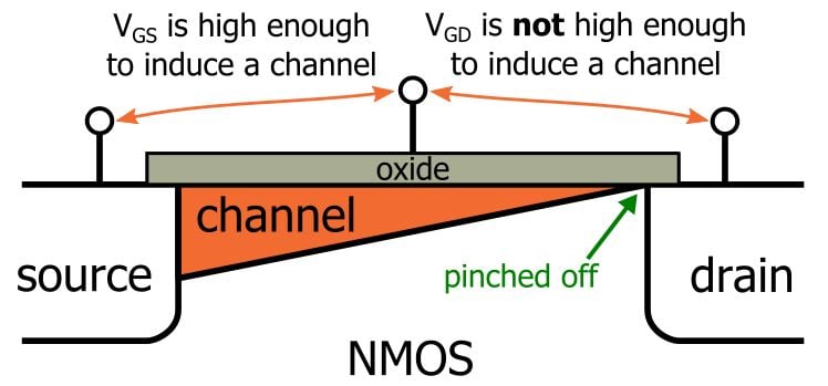
The transition to saturation mode occurs because the channel gets “pinched off” at the drain end:
Unfortunately, the “pinching off” isn’t the end of the influence exerted by the drain-to-source voltage. Further increases continue to affect the channel because the pinch-off point moves closer to the source:
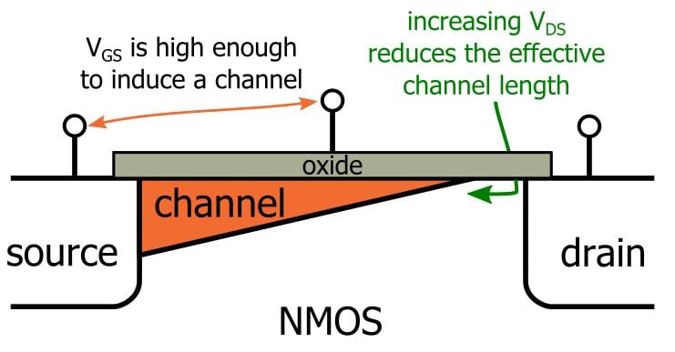
The resistance of the channel is inversely proportional to its width-to-length ratio; reducing the length leads to decreased resistance and hence higher current flow. Thus, channel-length modulation means that the saturation-region drain current will increase slightly as the drain-to-source voltage increases.
So we need to modify the saturation-region drain-current expression to account for channel-length modulation. We do this by incorporating the incremental channel-length reduction into the original expression:
$$I_D=\frac{1}{2}\mu_nC_{ox}\frac{W}{L-\Delta L}(V_{GS}-V_{TH})^2$$
(Note how the subtraction will reduce the denominator of the W/L term, leading to higher current.) By assuming that the incremental change is much less than the length of the physical channel (i.e., the distance between the source and drain regions), we can rearrange this as follows:
$$I_D=\frac{1}{2}\mu_nC_{ox}\frac{W}{L}(V_{GS}-V_{TH})^2(1+\frac{\Delta L}{L})$$
Now we just need to come up with a parameter that accounts for how a certain semiconductor process technology responds to changes in the drain-to-source voltage. How about we call this parameter lambda (λ), such that
$$\frac{\Delta L}{L}=\lambda V_{DS}$$
This brings us to our channel-length-modulation-compliant expression for saturation-region drain current:
$$I_D=\frac{1}{2}\mu_nC_{ox}\frac{W}{L}(V_{GS}-V_{TH})^2(1+\lambda V_{DS})$$
You might also see the following variant:
$$I_D=\frac{1}{2}\mu_nC_{ox}\frac{W}{L}(V_{GS}-V_{TH})^2(1+\frac{V_{DS}}{V_A})$$
where
$$V_A=\frac{1}{\lambda}$$
This modified drain-current expression is a first-order approximation that is reasonably accurate for FETs with channel length greater than, say, 2 µm. As the channel length decreases, so-called “short-channel effects” become more influential, and thus the above expression (which does not account for short-channel effects) becomes less valid.
Note also that the above expression incorporates the assumption that ΔL is much less than L; this assumption becomes less justifiable with shorter channel lengths, and indeed, researchers have developed a more sophisticated channel-length-modulation model for use with simulations involving modern short-channel devices.


when Vds is greater than Vdsat, then the channel shifts away from the drain. So, when there is no channel connection between source and drain, then how does the current reach drain?
Can anyone please explain this?