
 Facebook
 Google
 GitHub
 Linkedin
Industry White Paper
7 Things ASIC Architects Must Know About eFPGA Before Tape-Out
Embedded FPGA (eFPGA) is a block of reprogrammable logic built directly into an ASIC or SoC, so part of the chip’s hardware can be changed after it is manufactured. It has moved from an architectural luxury to a standard building block.
At 5nm and below, mask sets cost tens of millions of dollars, while mid-life protocol updates, post-quantum crypto standards, and late-stage lead-customer tweaks continue to threaten fixed-function silicon.
Before locking in your RTL, here are seven things to know about how eFPGA changes the silicon economics and integration flow for ASIC teams.
Image used courtesy of Freepik
1. eFPGA Eliminates the Standalone FPGA "SWaP-C Tax"
Off-the-shelf FPGAs carry general-purpose I/O, memory controllers, and SerDes interfaces that custom workloads rarely need. This imposes a size, weight, power, and cost (SWaP-C) penalty on every shipped board.
QuickLogic® eFPGA IP connects directly to the ASIC’s on-die AXI or proprietary interconnects. Because signals never cross chip pins or PCB traces, on-chip bandwidth increases dramatically while latency and high-swing I/O power drop. The ratio of Look-Up Tables (LUTs), DSP blocks, and Block RAM (BRAM) is tailored precisely to the ASIC’s target application.
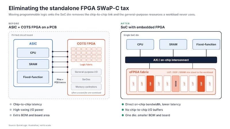
Figure 1. Moving programmable logic onto the SoC die removes the chip-to-chip link and the SWaP-C cost of general-purpose resources the workload never uses.
2. It Acts as "Silicon Insurance" Against Multi-Million-Dollar Respins
The traditional strategy of minimizing die area and deferring fixes to "Rev B" has become a high-stakes gamble. Between RTL freeze and volume ramp, standard specifications drift, and security vulnerabilities emerge.
Key Economic Calculation: Evaluating eFPGA is not a choice between IP license costs and zero cost; it is a calculation of IP Cost vs. Expected Respin Cost (Probability × Impact). Integrating a right-sized eFPGA block provides on-chip flexibility to absorb late-stage changes. Avoiding even a single respin routinely pays for the embedded logic core many times over.
3. Pre-Characterized Hard IP Removes Physical Implementation Risk
Delivering eFPGA as soft RTL transfers physical implementation burdens to the SoC team—including dense routing congestion, late-stage timing closure across tens of thousands of LUTs, and delayed IR-drop analysis.
QuickLogic delivers hardened eFPGA macros as fully characterized GDSII blocks accompanied by standard .lib timing models and power profiles across multiple PVT corners. It integrates into your floorplan with a fixed footprint, isolating internal fabric routing from the rest of the chip and reducing verification scope to the macro interfaces.
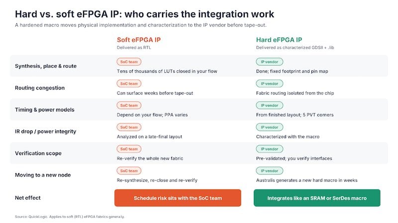
Figure 2. Soft (RTL) eFPGA leaves physical implementation, characterization, and per-node porting with the SoC team; a hardened macro moves that work to the IP vendor.
4. Timing Sign-Off Uses Your Existing STA Flow
Programmable logic does not require a novel timing methodology. QuickLogic simplifies static timing analysis (STA) by delivering dual IP timing views:
- Simple Mode: A conservative bounding-box model for early floor planning.
- Advanced Mode: A detailed, sign-off model characterized across five standard PVT corners (with custom corners on demand).
Boundary timing is closed outward by the SoC team using standard chip-level STA flows, while internal fabric paths are managed independently during bitstream compilation by QuickLogic’s software tools.
5. Automated Generation Tailors Logic to Any Node or Foundry
Unlike rigid, fixed-array blocks, QuickLogic’s Australis™ eFPGA IP Generator synthesizes custom hardened fabrics targeting specific process nodes and foundry PDKs in weeks.
- Foundry Flexibility: Silicon-proven and targeted across leading foundries, including Intel Foundry (Intel 18A, Intel 18A-P), GlobalFoundries® (22FDX®, 12LP), TSMC (N12e™, 22nm, 40nm), and UMC (22nm).
- Specialized Variants: Supports radiation-hardened-by-design (Rad-Hard) variants for space and defense applications.
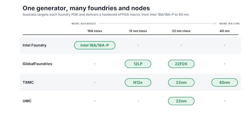
Figure 3. The Australis eFPGA IP Generator customizes eFPGA IP for any foundry and process technology.
6. Enables Field Reprogrammability for Post-Quantum Cryptography
Fixed-function crypto blocks cannot adapt to evolving threats without new silicon. By integrating QuickLogic eFPGA IP, SoCs gain true crypto-agility.
Through a collaboration with PQSecure Technologies and Xiphera, QuickLogic demonstrated post-quantum cryptography (CRYSTAL-1000C IP) running on eFPGA hard IP. Security logic, boot verification, and encryption algorithms can be updated post-silicon via secure bitstream updates.
7. Open-Source Tools Eliminate Vendor Lock-In for 30+ Year Lifecycles
Long-lifecycle defense, aerospace, and industrial programs require bitstream reproducibility decades after tape-out. Proprietary compiler flows risk obsolescence if vendor toolchains are discontinued.
QuickLogic’s Aurora eFPGA User Tools integrate fully open-source synthesis, place, and route modules. Development teams can inspect compiler source code, archive locked environment versions for bit-for-bit builds in 2055 and beyond, fork the toolchain if necessary, and satisfy Software Bill of Materials (SBOM) and supply-chain security requirements.
The Bottom Line
Post-tape-out specification changes are inevitable. By replacing unbounded respin exposure with predictable, hardened eFPGA IP, ASIC teams preserve optionality, accelerate time-to-market, and extend product lifecycles.
To learn more about QuickLogic’s Australis eFPGA IP Generator, Aurora open-source tools, or supported foundry nodes, visit www.quicklogic.com/efpga-ip or contact the QuickLogic eFPGA team.

