 Facebook
 Google
 GitHub
 Linkedin
Industry White Paper
Using Kikusui Multifunctional Electronic Loads in High Slew Rate Testing
This article is a walkthrough on leveraging multifunctional electronic loads and bias power supplies to expand the slew rate of a test setup. The combination of the equipment offered through Kikusui allows you to plan for high slew rate testing without worrying about the impact of negative voltages.
High slew rate testing with electronic loads is often necessary for applications such as load transient testing and battery and fuel cell testing. However, to successfully test with a high slew rate, it is essential to understand the impact of the inherent inductance of the test setup, i.e., the cabling, on the test. Employing a bias power supply allows you to upgrade the effective slew rate of your test, but some technical testing issues may remain.
This article is a walkthrough on leveraging multifunctional electronic loads and bias power supplies to expand the slew rate of a test setup.
The Need for High Slew Rate Tests
Testing with a high slew rate is necessary for several scenarios, including the research and development (R&D) phase of photovoltaic (PV) systems; the testing of battery electric vehicles (BEV) and hybrid EV (HEV) drives; and fuel cell, battery, and LED testing. A major test application that causes test engineers to consider slew rate is load transient testing of power supplies. Many supplies have demanding load behaviors and handle rapid changes in load current with minimal output voltage deviations. This situation is particularly true for the power delivery network (PDN) of application-specific integrated circuits (ASICs) or high di/dt converters.
Figure 1 shows how the transient specification depends upon the characteristics of the load step, or the momentary step up in current, and the output voltage response of the power supply. Characteristics of the load step include the minimum load during a transient event and the slope at the edges of the load step, i.e., the slew rate (often measured in A/μs). The transient response of the power supply reveals the maximum voltage deviation at both edges of the load step and the recovery time to reach the set voltage level.
![Figure 1: Load transient response of a power supply showing the load step in the output current and the respective changes in output voltage. Source [1]: Texas Instruments](https://www.allaboutcircuits.com/uploads/articles/image1_10.jpg)
Figure 1: Load transient response of a power supply showing the load step in the output current and the respective changes in output voltage. Source [1]: Texas Instruments
In Figure 2, you can see dynamic power profiles with detailed sequences adjusting current, voltage, and power. Over time, these are leveraged for stress testing to validate various battery models in BEVs and HEVs. Profiles such as the Federal Urban Driving Schedule (FUDS) and the New European Driving Cycle (NEDC) emulate real-world driving conditions. Performing these cycling tests over time allows designers to estimate failure rates and EV battery lifetime. These tests require both a power supply to exercise the complex driving cycles and a high slew rate load to effectively sink the current of the device under test (DUT).
![Figure 2: Power profiles for the dynamic stress test (DST), Federal Urban Driving Schedule (FUDS), New European Driving Cycle (NEDC), and real driving-1 (RD1) cycles. Source [2]: Baure and Dubarry.](https://www.allaboutcircuits.com/uploads/articles/image3_8.jpg)
Figure 2: Power profiles for the dynamic stress test (DST), Federal Urban Driving Schedule (FUDS), New European Driving Cycle (NEDC), and real driving-1 (RD1) cycles. Source [2]: Baure and Dubarry.
Electronic Loads in Slew Rate Testing
Contrary to conventional resistive and reactive (capacitive or inductive) load banks, programmable electronic loads use active circuitry to mimic changing load profiles. For all of these tests, it is necessary to have a reasonable electronic load with high power dissipation, a high load-current slew rate (di/dt), an adjustable load current, and load current monitoring to portray the behavior of a real load accurately. With all programmable loads, you can simulate the load profile with modes such as constant voltage (CV) and constant current (CC). You must understand how to handle the specific instrument employed in a test bench to meet the test requirements.
Bias Power Supply: Overcoming the Limiting Impact of Cables
Negative Voltage at the Electronic Load
The cable's inductance has a noticeable effect at high current slew rates. Figure 3 illustrates the inductor current and voltage relationship. This means if the cable inductance is 100 nH and the current flows at a slew rate of 30A/µs, then 3V (=100nH*30A/µs) is required at both ends of the cable—much larger than the 1V offered by the DUT. The connected electronic load in this test setup will not be able to output a negative voltage, causing test issues. More voltage is necessary through a bias power supply for this test to operate properly.
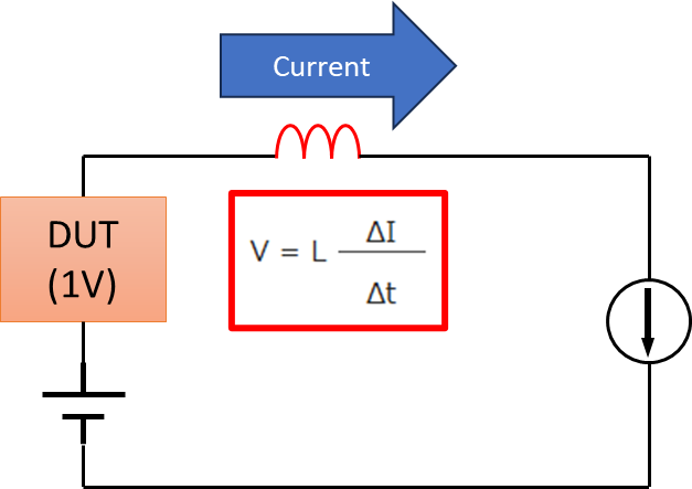
Figure 3: Simplified schematic showing how high slew rate currents may not flow due to voltage induced across the cable (a problem avoided by DC power supplies) because the electronic load cannot output negative voltage.
An example test setup using the Kikusui master PLZ1205W programmable electronic load, three PAT20-400T DC power supplies, and two ‘booster’ PLZ2405WB programmable electronic loads, which increase the total rated power of the setup, is shown in Figure 4. The simplified circuit diagram on the right of Figure 4 includes sample voltages. The DC power supplies a positive voltage output of 10V. The total voltage of the power supplies is combined with the DUT voltage (0.3V) and applied to the terminals of the electronic load to sink a total of 10.3V. Therefore, if a voltage drop occurs due to connected cabling or other potential factors, the electronic load can still draw current as the DC power supply is biasing the voltage. As a result, a positive voltage is always applied to the electronic load, preventing the high slew rate of the current from being reduced.
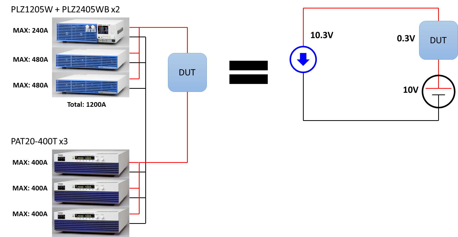
Figure 4: Sample test setup with the Kikusui PLZ1205W and PLZ2405WB multifunctional electronic loads and the PAT20-400T programmable regulated DC power supplies.
Increasing the Slew Rate
A test setup with the addition of a bias power supply (Figure 5) will increase the electronic load's effective slew rate. This increase results from the bias power supply’s ability to augment the current that the electronic load can draw.
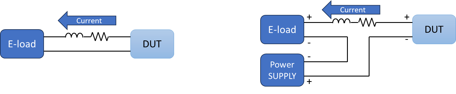
Figure 5: A test setup with a common electronic load (E-load) on the left and a system with a bias power supply on the right. The system with the bias power supply increases the slew rate of the electronic load.
For example, in Figure 4, the voltage of the DUT is 10 V, and the resistance of the cable is 0.1 Ω. Assuming the electronic load has a resistance of zero, the electronic load can theoretically draw up to 100 A (10 V/0.1 Ω). This current draw multiplies with the introduction of a bias power supply, meaning a 10 V power supply will increase the voltage applied to 20 V, thereby increasing the current that can be drawn to 200 A.
The slew rate can be calculated from the inductor current and voltage relationship, which is previously shown in Figure 3:

In this case, if the connected test cable is considered an inductance of 1 µH, the slew rate would be 20 A/µs (20V/1µH). For the test setup with an electronic load, the slew rate is 10 A/µs (10V/1µH). This basic example shows that using a bias power supply can exceed the upper limit due to the cables' physical characteristics.
Cabling Strategies
While adding a bias power supply reduces the considerations around the unwanted inductance offered by test cables, you still want to minimize the influence of cabling as much as possible. One method to do this is by twisting cables to reduce the total inductance. You can see this example in Figure 6, where a thick cable is required for a test setup with 1000 A of current running from the DUT to the electronic load. This same cable is routed from the master electronic load to its respective booster/slave units (PLZ405WB). If cabling is routed directly from the DUT to the electronic loads and the current splits between the paths, you can instead use a thinner, more twistable cable to reduce the overall inductance contributed by the cabling.
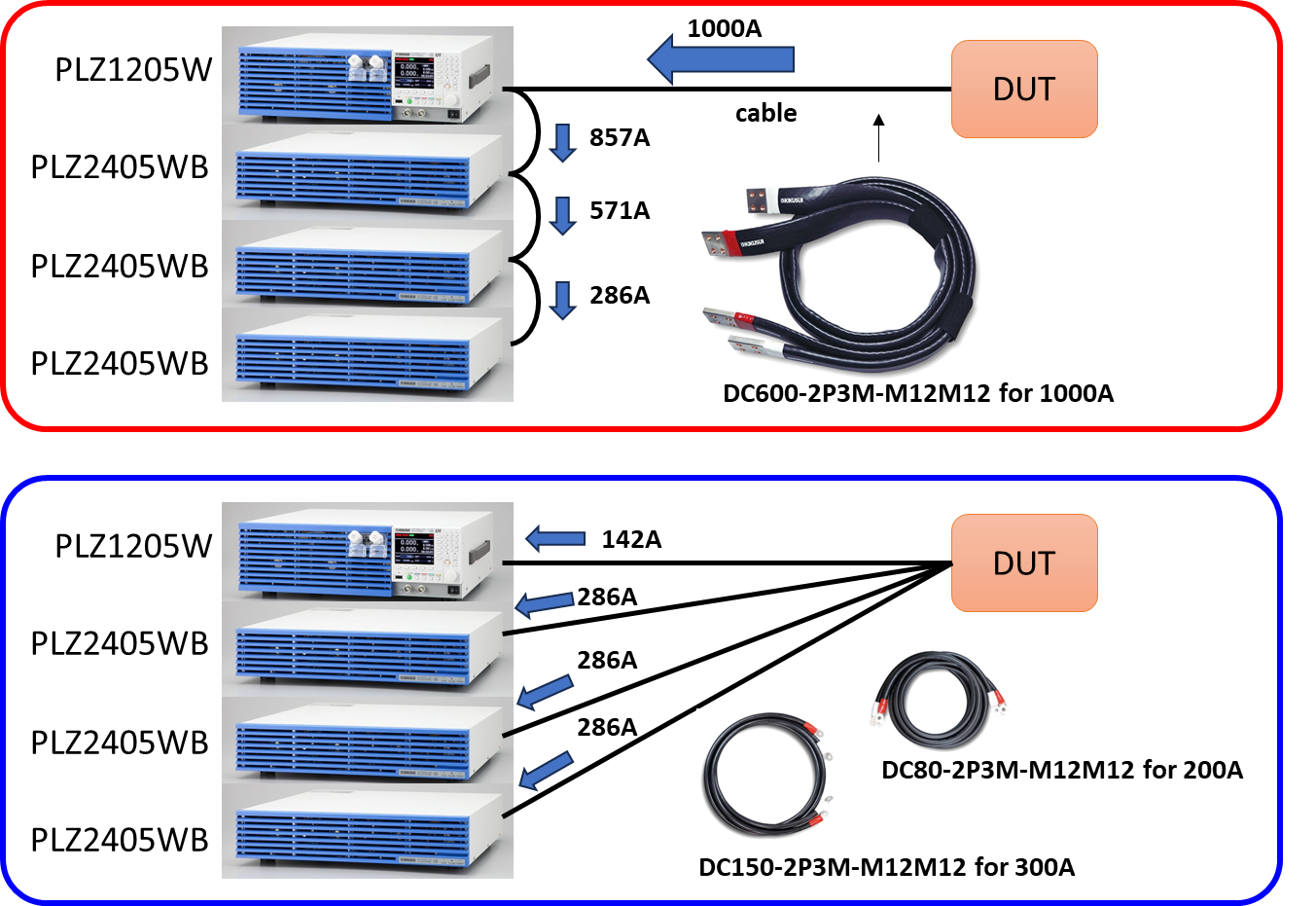
Figure 6: Test cabling layout routes where routing between the electronic loads will require you to use thicker cables that cannot be twisted (top), whereas routing between the DUT and the electronic loads will yield an overall reduction in current per cable and allow them to be twisted (bottom).
Avoiding Negative Voltages at the Power Supply
Introducing the bias power supply can cause a negative voltage to occur at the terminals of the DUT if there is a voltage drop due to DUT impedance variations. If a bias power supply provides 10V and an ideal electronic load (Voltage= 0V), then -10V can be applied to the DUT’s terminals. This may not be acceptable for many test scenarios. To bypass this issue, combine the remote sensing function and the under-voltage protection (UVP) function, where the electronic load is turned off if the voltage falls below 0V, protecting the DUT from negative voltages (Figure 7).
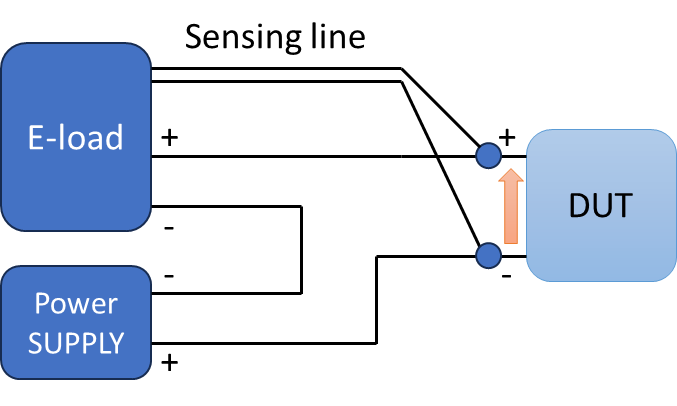
Figure 7: Adding a sensing line with combined remote sensing and UVP functions to turn off the electronic load if the voltage falls below 0V.
Nuts and Bolts: Building Out a High Slew Rate Test with Kikusui
It is important to follow certain guidelines to take full advantage of employing Kikusui equipment. This section outlines some of these key practices.
Layout Considerations
You can see the layout of the electronic load and bias power supply test setup in Figure 8. The negative terminal of the paralleled PWX1500L multi-channel rack-mounted power supplies must connect to the negative terminal of the paralleled PLZ-5W electronic loads. To parallel these instruments, it is essential to follow the recommended wiring diagram in the spec sheet.
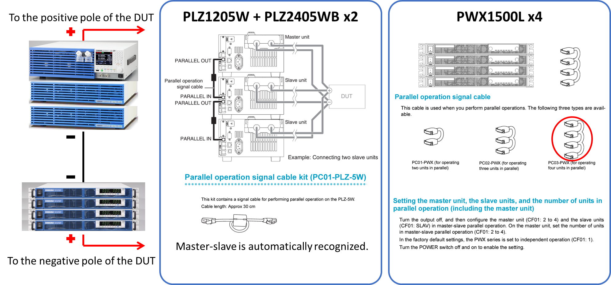
Figure 8: Instructions for paralleling the PLZ-5W electronic load and PWX1500L power supply (right) and connecting them in a test setup (left).
Terminal Considerations
Also, note that all specifications are intended for use with the rear terminals of the PLZ-5W electronic loads; using the front terminals may result in the test not meeting the intended requirements. Using the rear terminals can improve the slew rate. This can be seen in Figure 9, where the rise time in the current probe is decreased by using the rear terminals.
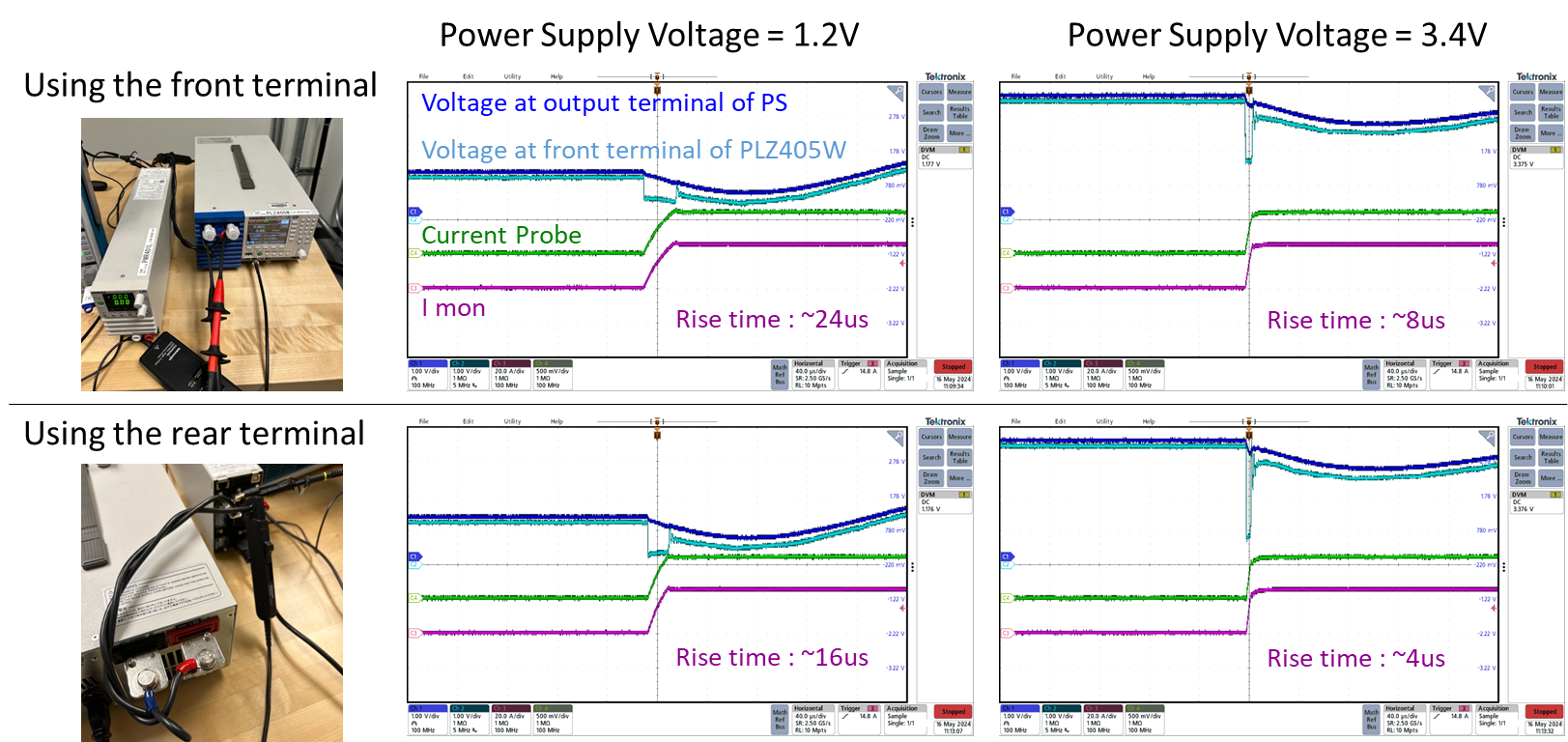
Figure 9: The rise time in the current is decreased by using the rear terminals of the PLZ-5W.
Slew Rate Considerations for Small Currents
Another factor to consider is the slew rate for small currents. The specified slew rate may not be achieved if the load current is too small in CC mode. The left-hand side of Figure 10 shows the current setting versus the logical current rise times and the actual current rise time when the slew rate is set to the maximum value in each range (H, M, L ranges). You can see that 31% of the PLZ1205W's H range (ratio of 75A to 240A = about 31%) shows a rise time of ~1 µs. The waveform on the right of Figure 9 signifies that the set slew rate of 60 A/µs is almost maintained for the slope.
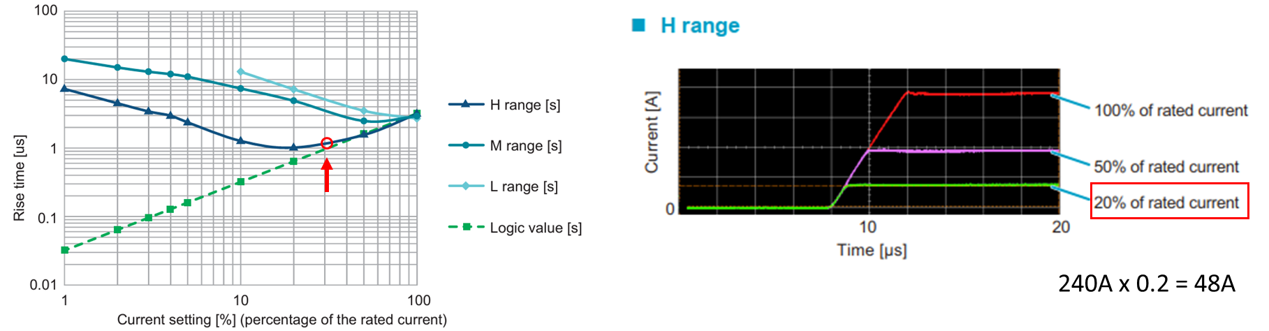
Figure 10: Example scenario showing that if the load current is too small in CC mode, the specified slew rate may not be achieved.
Conclusion
Building out a high slew rate test with electronic loads can be difficult due to the impact of inductance by test cables and the potential for a negative voltage to appear at the electronic load. To sidestep many of these issues, a bias power supply can be added to the test. This permits the electronic load to operate at higher slew rates and allows the total inductance contributed by the test cables to be brought down through careful test planning. Remember that introducing the bias power supply can potentially cause a negative voltage to appear at the DUT, and the solution to this issue is the connection of a sensing circuit.
Kikusui offers the PLZ-5W series of multifunctional electronic loads that, when paralleled together, can allow users to sink large amounts of power at a high slew rate. Kikusui also offers DC power supplies, such as the PAT-T series, with high current ratings. The combination of the equipment offered through Kikusui allows you to plan for high slew rate testing without worrying about the impact of negative voltages.
References
- “Load Transient Testing with High Slew Rates.” SSZTCV2 Technical Article | TI.Com, www.ti.com/document-viewer/lit/html/SSZTCV2. Accessed 10 Feb. 2025.
- Baure, G.; Dubarry, M. Synthetic vs. Real Driving Cycles: A Comparison of Electric Vehicle Battery Degradation. Batteries 2019, 5, 42. https://doi.org/10.3390/batteries5020042
