Facebook
 Google
 GitHub
 Linkedin
Image Sensors Suit up For AR/VR, Face Recognition, and More
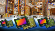
To serve the demands of a fast growing image sensor market, technology suppliers have rolled out innovative image sensor solutions, targeting AR/VR, face recognition, and autonomous cars.
The image sensor market is estimated to reach $26.1 billion in 2022 and grow to $38.6 billion by 2027, according to a report from market research firm MarketsandMarkets.
A key driver of this projection is the growing demand and adoption of image sensors in several applications, including Advanced Driver Assistance Systems (ADAS), machine vision in robotics, 3D motion sensors, and magnetic resonance imaging (MRI).
To feed those needs, several companies have rolled out new image sensor solutions this year to meet the growing demand and increasing adoption. In this article, we round up some of those image sensor advances.
Tiny Global Shutter Image Sensor
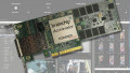
For its part, Omnivision offers its global shutter image sensor, the OGOTB, for augmented reality (AR)/virtual reality (VR)/mixed reality (MR) and Metaverse applications.

Functional block diagram for OGOTB from Omnivision. Image used courtesy of Omnivision. (Click image to enlarge)
This three-layer stacked image sensor offers the ultra-small form factor, low power consumption, and high image quality for face and eye tracking. The low power consumption and 400 × 400 resolution of the sensor make it well suited for small and lightweight battery-powered devices, says the company.
Omnivision says it incorporated several in-house technologies when developing this sensor, such as PureCel Plus, OmniBSI, and Nyxel NIR (near infrared). The OGOTB offers a 400 × 400 active array size, 2.2 μm × 2.2 μm pixel size, 1/14.46-inch lens size, 915.2 μm × 915.2 μm image area, 30.84-degree non-linear lens chief ray angle (CRA), 2.81 V analog and 1.1 V core power supplies, and an operating temperature range of -30°C to +85°C.

The OmniBSI capability in the OGOTB maximizes image quality in low-lighting conditions. Image used courtesy of Omnivision
According to the company, the OGOTB sensor offers programmable controls for cropping, mirror and flip, and frame rates, automatic black light calibration (ABLC), in-built strobe control, and multi-sensor mode operation. Developers can also make use of the device’s 8-bit/10-bit RAW output formats, horizontal and vertical 2:1 subsampling, and 1-lane MIPI/2-lane SPI serial output interface.
These features make the lens suitable for several applications, including industrial automation, biometric authentication, gaming, 3D imaging, drones, industrial bar code scanning, and ultimately to meet the requirements of AR/VR/MR devices, says Omnivision.
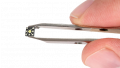
Behind-OLED Face Authentication Ref. Design
Another solution for today’s imaging system market comes from a collaboration between STMicroelectronics (ST) and Trinamix. The companies teamed up to develop a reference design for a face authentication system that original OEMs can implement behind the OLED screens of their products.
The reference design offers smartphone OEMs a solution that can integrate illumination, camera module, and high-performance processor-based algorithms. While ST supplies the camera module that combines the next-gen image sensor and NIR sensitivity, Trinamix supplies the patent-protected algorithm.
The resulting solution can enable high-security mobile payments due to its skin detection capability that can effectively differentiate human skin from fake presentations such as hyper-realistic masks, photos, and deep fakes.

STMicro and Trinamix teamed up to provide a “behind OLED” solution. Image used courtesy of Trinamix/BASF
The small, low cost, and high NIR sensitivity of ST image sensors make the face authentication system viable behind the display of smartphones since they offer compact sizes at high performance, say the companies.
Moreover, while the image sensors supply high sensitivity and low crosstalk capabilities for relevant applications, they deliver overall system integration, size, and performance improvements. They claim that the reference design assures OEMs the highest-efficiency face detection and next-gen performance due to the industry-leading pixel size capabilities of the image sensors from ST and the sophisticated processor-running algorithms from Trinamix.
The collaboration extends the support of the resulting solution to several applications, technologies, and ecosystems that serve the under-display market. This face authentication system is IIFAA, Android, and FIDO standard-certified for mobile payment applications. This makes it well suited to designing it into a wide range of smartphone devices, say the companies.
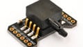
Silicon Image Sensor from Harvard Researchers
Growing demand for high-speed image processing in several applications, especially autonomous vehicles, is leading to the development of in-sensor processing.
In contrast to several past attempts at developing and demonstrating this processing technology, which has been challenging to incorporate into commercial systems, the in-sensor processor from Harvard University’s John A. Paulson School of Engineering and Applied Sciences (SEAS) leverages commercial silicon imaging sensor chip technology (CMOS) to capture and process visual information.
According to the researchers, this solution can significantly minimize the time it takes an autonomous system to identify an obstacle on its way and avoid a collision. Conventional autonomous systems take a snapshot of the object and deliver this data to a microprocessor for image processing. However, this in-sensor processor eliminates the extra step required to transmit the image for processing by ensuring real-time processing at collection.

Silicon photodiode array by Harvard SEAS researchers for in-sensor processing. Image used courtesy of Harvard’s SEAS
In their Nature Electronics paper, the SEAS researchers identified the solution as a foundation for in-sensor processing incorporation into several modern-day applications. The research team leveraged an electrostatically doped silicon photodiode array for image capturing.
Several Voltage Ranges
The doping ensures that operators can use several voltage ranges to tune the sensitivity of pixels or the photodiodes to incident light rays. The resulting voltage-tunable photodiodes can achieve several computational operations for real-time image capturing and processing.
With this solution, say the researchers, image systems in autonomous vehicles can promote passenger and driver safety through high-accuracy lane marking tracking with high-pass filters. Similarly, image systems in other applications can ensure high-image quality through noise reduction blurring by implementing this solution.