Facebook
 Google
 GitHub
 Linkedin
Considerations for Adding Reset Capability to an FPGA Design
This article will look at some of the consequences of adding a reset input to an FPGA design.
This article will look at some of the consequences of adding a reset input to an FPGA design.
This article will review some basic considerations for coding a given functionality with a reset input. The consequences of using a reset input may be overlooked by the designer but an improper reset strategy can easily impose heavy penalties. Reset capability can adversely affect the speed, area, and power consumption of an FPGA design.
Before proceeding with our discussion, it’s worth to emphasize on one basic principle: FPGAs are programmable devices but this doesn’t mean that we can program every feature in an FPGA. This basic principle will be further clarified in the rest of the article.
Carefully Read the Details Before You Add a Reset Input
Figure 1 shows a D-type flip-flop (DFF) which is available in the Xilinx 7 series FPGAs.
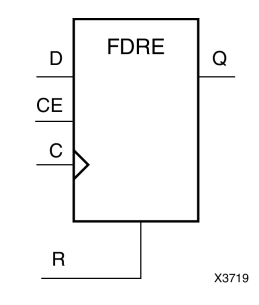
Figure 1. FDRE D-type flip-flop of the Xilinx 7 series FPGAs. Image courtesy of Xilinx.
This particular DFF, which has a synchronous reset (R) and a clock enable (CE) input, is called an FDRE (Flip-flop, type D, synchronous reset, with clock enable) in the Xilinx Library Guide. The logic table of this element is shown in Figure 2.
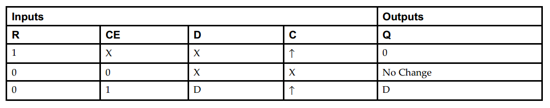
Figure 2. The logic table of FDRE D-type flip flop of the Xilinx 7 series FPGAs. Image courtesy of Xilinx.
Here, R, CE, D, and C are the inputs of the DFF and stand for reset, clock enable, data input, and clock, respectively. X represents a “don’t-care” and ↑ denotes the clock rising-edge. The reset is synchronous because it can reset the output only at the rising edge of the clock.
This DFF is a design element that can be used as a building block of a larger design. We can use it to register a desired signal. And, we are free to use the reset and clock enable inputs of the FDRE as we want.
We can choose if we want to use an available feature of a building block or not. However, we cannot add an unsupported feature to a given building block. As an example, consider the FDRE element discussed above. This design element only supports a synchronous reset. In case we need both asynchronous and synchronous resets, we won’t be able to use the FDRE flip flop. In this case, the synthesis tool will have to use another resource or it may even resort to using a combination of the available building blocks to realize the desired design. As you can see, the low-level features of the FPGAs are fixed but once these design elements are configured, we connect them together the way we want and build a larger design.
As a more subtle example of how the FPGA granularity can affect the implementation, note that, according to the above logic table, the reset (R) input of the FDRE has a higher priority relative to the clock enable (CE) input (notice on the first line of the table that when R is 1, CE is irrelevant). Now, assume that our HDL code uses a DFF with both reset and clock enable inputs. And, the HDL description gives the higher priority to the CE input rather than the R input. Again in this case, the synthesis tool will have to use a resource other than the FDRE or it will have to use a combination of the available building blocks to realize the desired functionality. For more details about this example, refer to this Xilinx white paper.
The above discussion shows that, to have an efficient design, we have to carefully study the details of the FPGA design elements just as we study the datasheet of a discrete component before using it. In the rest of the article, you’ll see some other examples of this principle.
Shift Register Lookup Table (SRL16)
The Xilinx synthesis tool can realize LUT-based shift registers that are much more compact and faster than the structure obtained from simply cascading some DFFs. These efficient shift registers, called SRLs, don’t support a reset input. That’s why, if your shift register doesn’t really need a reset, you should avoid it so that the synthesis tool is allowed to infer an efficient SRL-based realization for the shift register. If your code describes a shift register with reset, XST will implement the design using DFFs or it will use some additional logic around the SRL to allow a reset functionality. SRLs can be inferred from simple concatenation operators (See page 154 of the XST User Guide).
Block RAMs
Similar to the case of SRLs, we cannot reset the content of a block RAM using an explicit reset. That’s why when mapping a design into block RAMs, we shouldn’t use a reset. You can find some more details here.
Multipliers
Unlike an SRL or a block RAM which doesn’t support a reset, some modules, such as multipliers, have limitations for the type of the reset. These modules only support a synchronous reset. For a given multiplier, replacing an asynchronous reset with a synchronous strategy can increase the frequency of operation by a factor of two or more.
To summarize, an improper reset strategy prevents the synthesis tool from efficiently utilizing the optimized modules available in the FPGA. This can adversely affect area, power, and speed of a design. Now, let’s see some examples where the synthesis software uses the reset port of the DFFs to perform some optimizations.
Use of Set/Reset Inputs to Optimize the Implementation
It’s usually recommended to avoid use of set and reset inputs as much as possible. This helps the synthesis tool to apply an optimization where the set/reset inputs of the DFFs are examined to simplify the implementation. To further clarify, assume that we want to implement the schematic shown in Figure 3.
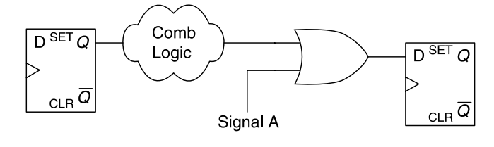
Figure 3. A particular case that can be optimized by the synthesis software. Image courtesy of Advanced FPGA Design.
In Figure 3, when “Signal A” is logic high, the DFF output will go high at the clock edge no matter what the output of the combinational circuit “Comb Logic” is. That’s why, as shown in Figure 4, the synthesis software can eliminate the OR gate and apply “Signal A” to the synchronous set input of the DFF. Now, when “Signal A” is logic high, the DFF will be set to high at the clock edge. Otherwise, the output will be determined by the combinational circuit “Comb Logic”. The new design gives the desired functionality but, now, the OR gate is eliminated and both speed and area of the design can be improved.
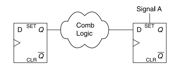
Figure 4 .The optimized form of the circuit in Figure 3. Image courtesy of Advanced FPGA Design.
It’s interesting to note that, sometimes, the synthesis tool may decide to do the reverse of the above optimization and implement the schematic of Figure 4 as shown in Figure 3! This is due to the fact that, in 7 series, all the DFFs in a slice share the same CK, SR (set/reset), and CE signals. This means that a DFF whose SR input is connected to “Signal A” cannot be in the same slice which has a DFF with its SR input connected to a signal other than “Signal A”. If the control signals, i.e. CK, SR, and CE, are not the same, the DFFs must be placed in different slices. This can lead to an inefficient slice utilization in a design which uses many low-fanout reset signals. In fact, each low-fanout reset signal will use a few DFFs of a slice and the remaining DFFs of the slice will be wasted. In such cases, the synthesis tool can implement the schematic of Figure 4 as shown in Figure 3. This process will lead to DFFs that don’t use their reset inputs. As a result, these DFF can share the same control signals and can be placed in the same slice. Therefore, the device utilization will be improved.
In Figures 3 and 4, we saw that an OR gate followed by a DFF can be replaced with a DFF which uses its set input. Similarly, we can replace an AND gate followed by a DFF with a DFF which uses its reset input (See Figure 5 below).
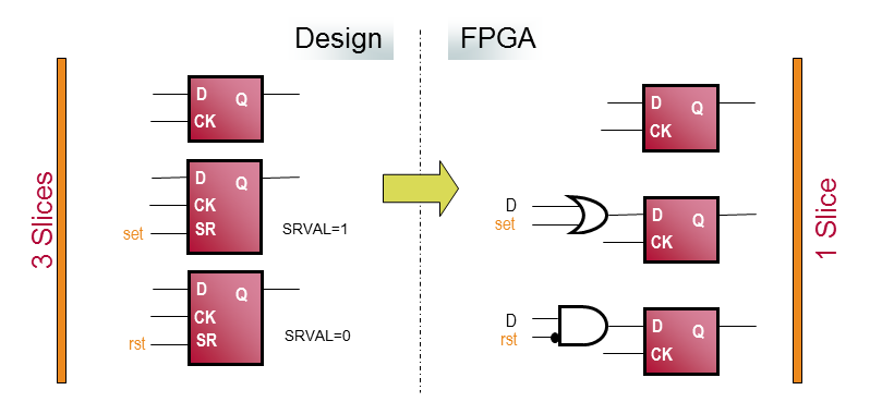
Figure 5. Image courtesy of Xilinx.
In Figure 5, the SRVAL attribute specifies the output value of the DFF after asserting the SR input. Therefore, for the middle DFF on the left, the SR input is specified as a set port. However, for the lower DFF on the left, the SR input is actually a reset input. The upper DFF doesn’t use a reset input.
The three DFFs on the left cannot be placed in the same slice because they have different control signals. However, with the conversions discussed above, we obtain three DFFs with the same set of control signals. Hence, we can put the three DFFs in the same slice. Note that the above conversions are not valid with asynchronous set/reset signals. That’s why we are usually recommended to use synchronous set/reset signals rather than asynchronous ones.
References
- How do I reset my FPGA? by Srikanth Erusalagandi, Xilinx.
- Get your Priorities Right – Make your Design Up to 50% Smaller by Ken Chapman, Xilinx.
- Advanced FPGA Design: Architecture, Implementation, and Optimization by Steve Kilts.
- HDL Coding Practices to Accelerate Design Performance by Philippe Garrault, Xilinx.
- Get Smart About Reset: Think Local, Not Global by Ken Chapman, Xilinx.
To see a complete list of my articles, please visit this page.
Related Content