 Facebook
 Google
 GitHub
 Linkedin
PCB Layout Style Mistakes That Can Ruin Your Design
This article discusses style mistakes in PCB layout that can make assembly and debugging PCBs difficult. This is vital for designers!
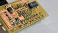
Sloppy Layout = Lots of Problems Later
Modern PCB layout software allows engineers, designers, and hobbyists to quickly and easily design PCBs. The software provides the freedom to be creative, but sometimes that’s not a good thing. PCB designers can make sloppy design mistakes that don't impact the product functionality, but may impact assembly, debugging, and yield because of the confusion these sloppy mistakes cost. This article covers some of the basic sloppy PCB design style mistakes and how to avoid them.
Reference Designator Under Pads
Reference designators placed on a copper show up in PCB layout software, but not on a physical PCB. If your reference designators are placed on pads in layout, they’ll be missing when you get your PCB, and placing components will be difficult. In the picture below, the reference designator for R1 will not be printed completely on the PCB. The "1" will be clipped. The reference designator for R2 is placed correctly.

Reference Designator Under a Package
If you place a reference designator under a component, you or your contract manufacturer may be able to place the component, but it will be hard to find the component on the PCB if you need to remove or replace the component for repair or debugging. In the picture below, the reference designator for U1 will be hidden after U1 is placed on the PCB. The reference designator for U2 will be clearly visible after U2 has been placed.

Reference Designator Not Clearly Assigned to Components
Place reference designators as close as is practical to their components. Place the reference designators in a way so that it is clear which components they belong to. Not doing this makes it hard to place the correct components in the correct place. This is important for assembly and debug. In the picture below, it's not clear which resistor is R1 and which is R2.

Reference Designators in Small Font
Use a font for reference designator that is large enough to easily read. The author has had success with fonts that are at least 0.060” tall and 0.050” wide. This tip doesn't get a picture because reference designators of any size can look good on a large, high resolution monitor, especially when you're zoomed in.
Components Close To Each Other With Ambiguous Reference Designators
Components placed next to each other where the reference designators don’t clearly indicate which components go on which pads can result in a multitude of problems including the wrong components being placed on the wrong pads or components being placed in a way that wasn’t intended that introduces short circuits or open circuits. The author has seen layouts with this mistake as illustrated in the picture below. Some of the PCBs made with this layout were assembled correctly with the resistors placed horizontally. Other PCBs were assembled incorrectly with the resistors placed vertically. This misplacement of parts caused the PCBs not to work.Using footprints that have outlines around the components is a way to avoid this problem.

Reference Designators With Random Orientation
Reference designators on a PCB should face one or at most two directions. Randomly oriented reference designators makes assembly and debug more difficult as components are more difficult to find. The components on the left have reference designators placed appropriately. The components on the right have reference designators with different orientations, which is bad.

Not Labeling Pin 1 on Integrated Circuits
Integrated circuits should have a clear indicator, like a dot or a star, next to pin 1 to make sure the IC is installed properly. Improperly installed ICs will likely be damaged or destroyed. Debugging will be easier if the pin 1 indicator is not buried underneath the IC when the IC is on the PCB. In the picture below, U1 will be difficult to place correctly. Note that that the pin numbers you see in the picture won't be on the PCB. U2 will be placed correctly because pin 1 is clearly marked (the square pin).

Not Labeling Polarity for Polarized Components
Some two-terminal components like LEDs and electrolytic capacitors are polarized. Installing polarized components incorrectly can cause circuit malfunction or component destruction. LEDs provide light only when installed properly. If installed backward, LEDs will not conduct, and may even be damaged by voltage breakdown. Electrolytic capacitors explode if reverse biased. Use footprints that indicate polarity. Polarity markers should not be buried under the component. In the picture below, C1's package is not good because the polarity marker will be covered up by the component. C2's package is good because the polarity marker will be visible when the capacitor is on the PCB.

Placing Components Too Closely Together
Placing components too closely together can cause issues like solder bridges. If components are too close, they may be difficult to probe with an oscilloscope or multimeter, as the probe may short multiple components together. Placing components too closely together can also make replacing components difficult. This is best seen on a PCB, as component spacing may look ok on a large monitor.
Not Using Thermal Relief
Use thermal relief on component pins to make soldering easier. You may be tempted to not use thermal relief to reduce electrical and thermal resistance, but not using thermal relief can make soldering very difficult, especially when a component pad is connected to a large trace or copper fill. Large traces and copper fills act as heatsinks that can make heating the pad for soldering difficult if properly thermal relief is not used. In the picture below, there is no thermal relief on the source pin of Q1. This MOSFET may be hard to solder and desolder. The source pin of Q2 is thermally relieved. This MOSFET will be easy to solder and desolder. PCB designers can change the amount of thermal relief to control electrical and thermal resistance of the connection. For example, a PCB designer could lay traces over the Q2 source pin to increase the amount of copper connecting the source to the ground node.

Know PCB Manufacturer, Contract Manufacturer, and Your Limitations
Have a good set of design rules that your PCB manufacturer can meet.
Know if you or your CM can handle difficult packages like ball grid array. If you are doing your own soldering, packages with legs that stick out to the side of an IC package are easiest to solder, especially if the pitch isn’t too small (less than 0.100”).
Conclusion
This article has covered some of the PCB layout style issues that can cause problems with assembly and debugging. Remember to carefully place reference designators, use good footprints with polarity and pin 1 marks, use thermal relief, and designing with manufacturing limitations in mind. Following these good design practices will make assembly easier, improve yields, and make for easier debugging. These benefits all save time and money and promote peace of mind.
Related Content


Great tips, thank you. It’s good to have a formal list of guidelines. That way, if the occasion comes up where a rule needs to be bent, it’s done with full understanding of what is at stake.