
 Facebook
 Google
 GitHub
 Linkedin
5 V MCUs and 5 V Tolerant MCUs—What’s the Difference and Why It Matters
5 V microcontrollers vs. 5 V Tolerant microcontrollers: That single word is a massive differentiator. Learn the crucial difference between supply voltage and I/O tolerance for predictable 5 V logic design.
Reading microcontrollers (MCU) specifications is like being a lawyer—verbiage is everything. Take the difference between the phrases “5 V MCU” and “5 V Tolerant MCU.” That single word, “tolerant,” is a massive differentiator between devices.
A 5 V MCU is a device that can run on a supply of 5 V, whereas a 5 V tolerant device is a device that can merely tolerate 5 V logic applied to an I/O pin. This distinction may seem minor, but it is a crucial parameter to understand when designing with 5 V logic.
While the world is transitioning towards lower voltage logic (3.3 V, 1.8 V, 1.2V , etc.) 5 V still remains commonly used because of its large signal margins. These signal margins determine the point at which a signal is guaranteed to be received as a “1” or a “0.” Below this region, the behavior is not predictable. A simple diagram of the valid states is shown in Figure 1.
An MCU Example
As an example, let’s assume that for a specific MCU to guarantee that it receives a LOW (0) and HIGH (1), the microcontroller needs to see ≤ 20% of the supply voltage (VDD) for LOW and ≥ 80% of VDD for HIGH. In this scenario, 5 V logic has a margin of 1 V, before considering other losses. For comparison, 3.3 V logic has a margin of 660 mV in this example.
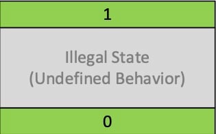
Figure 1. Digital logic states for I/O pins
But, what if 5 V was applied to a normal 3.3 V input? Wouldn’t that solve the problem?
The reason why this is problematic is due to the Electro-Static Discharge (ESD) protection circuitry inside of an I/O pin. ESD circuits steer surges into the power rails, where they can be absorbed or mitigated. Normally, the I/O voltage is less than a diode drop (0.7 V) from either the positive supply or ground, so the diodes are effectively not in circuit. This is shown in Figure 2.
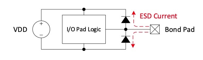
Figure 2. Simplified schematic of I/O pad
However, if the voltage applied to an I/O is higher than this diode drop, then the diodes will steer the signal into the power rail, like an ESD surge. This can have additional knock-on effects such as pulling the power rail up and pulling a lot of current from the outputting device. If the IC wasn’t powered on when an active HIGH signal was connected, the chip itself can even power-up from the I/O pin supplying current through the diode.
All About ESD Structure
So, how do designers get around this problem when making 5 V tolerant I/O? The trick is in the ESD structure—rather than implement a single diode, like normal, the designers can implement multiple diodes in series or use a Zener diode instead. Either way, the diode(s) are designed not to conduct at the slightly higher voltage on the I/O pin.
But, since ESD surges are much, much higher voltage than any normal operating voltage, these surges are still safely directed to the power rails. One limitation of this trick is that while the device can receive 5 V logic, it cannot generate it directly, as the I/O rail is still referenced to a different voltage domain.
A simple workaround, if the signal is slow enough, is to use a resistor and transistor in an open drain configuration as shown in Figure 3. The 5 V pull-up generates an idle 5 V rail, and when the MCU asserts a logic HIGH, the transistor pulls the line LOW.
This has the unfortunate side effect of acting as an inverter, however, and has poor slew rate performance due to the slow recharge of the capacitance of the I/O line. Additionally, driving the line low pulls current constantly through the resistor, which can be a non-trivial source of power drain for a battery powered application.
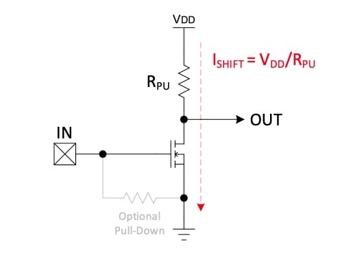
Figure 3. Schematic of a simple level shifter
A better-performing alternative level-shifter is to buy a dedicated logic level translator IC. However, this adds to the BOM and requires designers to match the required I/O directions (for example, 2 out, 2 in) to the functions on the translator (for example, 2+ out, 2+ in). Using a true 5 V MCU would remove all the headaches above.
Two Different Voltage Domains
But what if there was a way to have two different voltage domains in the microcontroller at the same time? This is a scenario where the Multi-Voltage I/O (MVIO) peripheral becomes quite useful. For instance, imagine an industrial controller where the UART to/from the outside world is 5 V, but the logic inside the assembly is 3.3 V. A 5 V MCU can’t interface with the 3.3V devices since the I/O would be 5 V referenced.
MVIO is a hardware peripheral that enables an MCU to have an I/O bank supplied independently from the core. So, in the above example, the MVIO bank could be powered at 5 V, while the rest of the MCU runs at 3.3 V. All the required I/O level translation occurs in the I/O pads of the MCU with no extra area, costs or hassles.
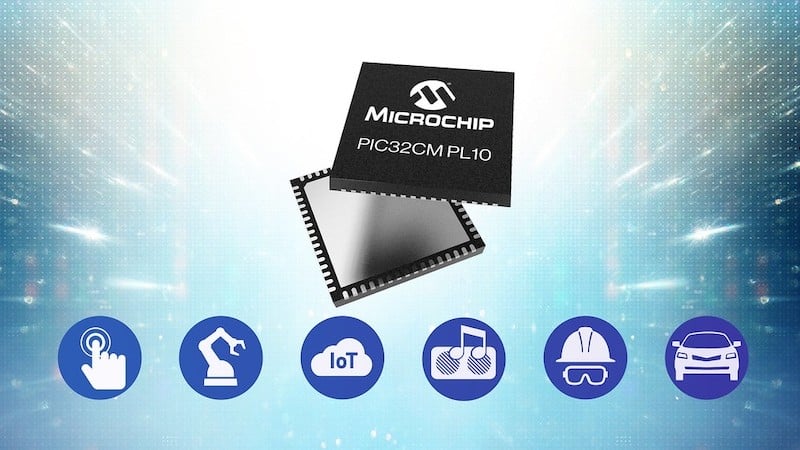
Figure 4. Microchip’s PIC32CM-PL10 microcontroller
MVIO also can work in reverse, such as a 5 V MCU with a dedicated 3.3 V (or lower) I/O bank. MVIO was first introduced on the AVR DB family of MCUs but is now available on 32-bit products such as the Microchip PIC32CM-PL10 MCUs (Figure 4). The PL10 is a 1.8 V to 5.5 V MCU containing an Arm Cortex-M0+ CPU at 24 MHz with a built-in water-resistant capacitive touch controller.
The PL10 family of MCUs is pin-to-pin compatible with the AVR Dx [for example, DA, DB, DD] families of MCUs for an easy upgrade path, and this combination of features allows PL10 MCUs to be used in a wide variety of applications and operating ranges.
Trend Toward Lower Voltages
Back to the industrial controller example. If 5 V logic is so useful, why can’t everything use it? The reason why more and more modern electronics are trending to lower voltage domains is due to higher power efficiencies, higher clock speed requirements and miniaturization of semiconductors. For instance, the power loss from an (ideal) switching CMOS circuit can be estimated with the following formula:
$$P_{SW} = \frac{1}{2} CV^2\times f_{CLK} \times \alpha$$
Where C is the capacitance of the CMOS circuit, V is the operating voltage, f is the clock frequency and α is the clock activity factor. For a constantly switching clock signal, α = 1. From this formula, it’s clear that decreasing the logic level voltage provides an exponential savings in power loss. However, it should be noted that in systems where the clock frequency is low or not very active (α << 1), the benefits of this transition are lower.
So, in summary, a 5 V tolerant MCU is a device where the ESD structure has been engineered and tuned to withstand the higher voltages applied to the input. By contrast, a 5 V MCU is a device that can run on a 5 V supply. Understanding the difference between the two is important to ensuring signals are received correctly, and the design functions as expected.
All images used courtesy of Microchip.











Good explanation