Facebook
 Google
 GitHub
 Linkedin
Decisions Ahead for the Next Generation of Advanced Packaging
Advanced packaging is at a crossroads due to AI demand. Learn the four emerging paths—CoWoS, CoPoS, glass-core, and CoWoP—and how to choose the right one for your multi-die system design.
The wild enthusiasm for large language models (LLMs) is driving an explosive expansion of AI-scale data centers. New installations and planned sites seem to appear everywhere at once. Along with this buildout comes intense pressure for ever more compute, lower energy per inference, and higher reliability at the rack level.
Server boards that deliver this performance rely on GPUs, AI accelerators, and CPUs. Those devices have evolved from single monolithic chips to multi-die systems assembled with advanced packaging. Now, the same pressure that created multi-die systems is pushing those assemblies to become larger, hotter, and more complex.
For these systems-in-package (SiPs), the performance characteristics that matter to data center operators—bandwidth, latency, power, and reliability—are increasingly dominated not by the dies themselves but by the advanced packaging technology that carries, interconnects, and cools them.
This pressure is forcing advanced packaging to show a credible roadmap that supports more dies, higher speeds, and continued control over thermal and mechanical issues.
A Fork in the Road
As that roadmap comes into focus, it is becoming clear that there is no single path to a more capable future. Instead, we are approaching a fork in the road with several distinct branches. Each path has its own strengths and weaknesses. Each will influence both the system partitioning and the supply chain for GPUs, accelerators, and CPUs that follow it. System designers must understand their options and make packaging-aware decisions early in the design planning process.
This article compares four directions that are now emerging as serious candidates:
- Extending CoWoS.
- Moving to CoPoS, a panel-level fan-out evolution of CoWoS.
- Introducing glass-core panel substrates.
- Skipping the organic substrate with chip-on-wafer-on-Platform-PCB (CoWoP).
Rather than searching for a single winner, we will examine where each option is likely to fit and how design teams can preserve optionality as the ecosystem evolves.
CoWoS: Proven, But Constrained
Today, multi-die AI accelerators with HBM are built primarily on chip-on-wafer-on-substrate (CoWoS). A silicon interposer is fabricated on a 300 mm wafer using conventional front-end and back-end processes. This interposer provides dense redistribution layers (RDL) for thousands of fine-pitch connections between a logic die and multiple HBM stacks, as well as through-silicon vias (TSVs) to carry power and signals down to an organic substrate.
The flow is familiar: dies are placed and bonded on the interposer wafer, the wafer is diced into large rectangular interposers, and the waste area at the circular edge is discarded. The die-interposer assemblies are then mounted on a high-performance organic substrate—commonly based on Ajinomoto Build-up Film (ABF)—which serves as a coarse redistribution layer and provides the solder bumps that connect to the PCB: a heat spreader and cooling solution on top complete the stack.
This architecture naturally creates three classes of interconnect:
- Very fast and dense on-die wiring.
- Somewhat slower and less dense interconnect on the silicon interposer
- Relatively slow and sparse routing in the organic substrate and PCB.
It is up to the system architect to juggle these domains—partitioning functions across dies and deciding which signals stay on-die, cross the interposer, or traverse the substrate—to meet bandwidth, latency, and power targets.
CoWoS has been in production for years and is considered a mature, low-risk technology. It is the foundation for most of today’s flagship AI accelerators and high-end networking ASICs. The first constraint, however, is interposer size. In mainstream CoWoS-S, the interposer is limited by the reticle's exposure area. Current offerings support interposers up to three times the reticle size, on the order of 2700 mm². Beyond that roughly 2700 mm² range, more complex schemes such as CoWoS-L or CoWoS-R are required, adding process complexity and cost.
The second constraint is geometry. We are cutting large rectangular shapes from a circular wafer. Even with careful die tiling, a significant fraction of the wafer edge area cannot be used as usable interposers. In practice, only about two-thirds of the theoretical wafer area converts into large, high-quality interposer dies.
The result is a technology that is functionally excellent but capital-intensive and capacity-constrained. Foundries have invested heavily to increase CoWoS output, but demand from AI accelerators and other multi-die systems continues to catch up. For many programs, the question is not whether CoWoS is technically suitable, but whether it will be available in the right volume, at an acceptable cost, and on a satisfactory schedule.
CoPoS: Another Path
One proposed successor is chip-on-panel-on-substrate (CoPoS), a panel-level fan-out packaging technology. Conceptually, CoPoS extends the CoWoS idea to a rectangular panel rather than a round wafer. Panel sizes on current roadmaps range from roughly 300 × 300 mm to around 500 × 500 mm, depending on the supplier and process. (Figure 1).
From a system perspective, the main advantage is area utilization. Large rectangular devices tile naturally on a rectangular panel, with far less dead area than on a circular wafer. For ultra-large AI packages that approach the limits of CoWoS-S, this extra usable area directly translates into more packages per carrier and a lower cost per square millimeter of “useful” interposer or fan-out region.
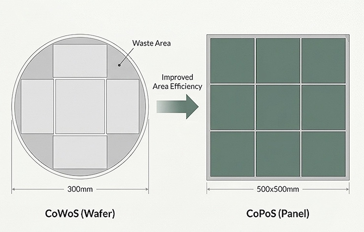
Figure 1. Comparing the area utilization of CoWoS and CoPos
Panel-based processes on organic or glass carriers have already demonstrated redistribution layers with line/space in the 3–5 µm range, with development work pushing toward finer geometries. This is not yet as aggressive as the most aggressive silicon-interposer wiring. Still, it is sufficient for many HBM-on-logic topologies if bump pitch and interface width are chosen carefully.
The trade-off is maturity. CoPoS requires new tools, new materials handling, and new yield learning. Public roadmaps and industry reports describe pilot lines in the middle of this decade and mass production closer to the end of the decade. That makes CoPoS a medium-term option: attractive for designs that need vast fan-out areas and can align their launch windows with that schedule, but not yet a drop-in replacement for near-term, high-risk flagship products.
Glass-Core Panels: Upgrading the Substrate
In parallel, the substrate industry is working on glass-core panel substrates. Compared with organic cores, glass offers several attractive properties:
- Superior dimensional stability and lower warpage, which help alignment and yield on large panels.
- Low dielectric loss, significant for multi-gigabit and multi-tens-of-gigabit links.
- The potential for fine-pitch RDL on both sides of the core, plus through-glass vias (TGVs) to connect them.
Equipment and materials vendors have reported roadmaps for glass substrates with line/space moving into the low-micron range, along with panel sizes similar to those discussed for panel-level fan-out. In effect, glass cores can bring some “interposer-like” routing density into the substrate itself. (Figure 3.)

Figure 2. Table comparing the use of glass core in the substrate with alternative materials. (Click on image to enlarge).
For system and chip designers, glass opens several scenarios:
- Reducing or eliminating the need for a separate silicon interposer in some 2.5D assemblies by shifting more routing into the glass core.
- Combining panel-level fan-out on top of a glass core to build very large AI or networking packages without pushing CoWoS-S beyond its comfortable range.
- Enabling low-loss, high-frequency paths for chiplets, SerDes, or RF functions at the package level.
Glass is not a free upgrade. It demands different forms of formation, other handling and reinforcement, and new inspection strategies. Existing organic-core lines are well amortized and will remain attractive for many products. In practice, glass is likely to appear first in the highest-end, most bandwidth-hungry systems and then gradually diffuse into broader markets as volumes grow and costs fall.
CoWoP: Collapsing Package and Board
Chip-on-wafer-on-Platform-PCB (CoWoP) is the most disruptive of the four options. Here, instead of mounting the silicon interposer or fan-out assembly on an organic package substrate, the entire structure is attached directly to a high-density printed-circuit board. (Figure 3.) The ABF or BT substrate disappears from the stack.
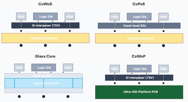
Figure 3. Chip-on-Wafer-on- Platform-PCB (CoWoP)
To make this feasible, the PCB must become much more like a substrate. Ultra-HDI boards with line/space in the 15–20 µm range, multiple lamination cycles, and carefully engineered materials to control warpage and CTE are required. This is a significant stretch from today’s mainstream server boards, but not out of reach as PCB technology advances.
If CoWoP can achieve stable yields on large interposers or fan-out assemblies mounted directly onto boards, it offers a simple story: fewer layers, fewer assembly steps, and a shorter path from silicon to system. It would also shift more value and innovation to PCB manufacturers, potentially changing the structure of the advanced-packaging supply chain.
The risk is that CoWoP compresses several challenging problems—fine-line PCB manufacturing, flatness on large boards, high-current power delivery, and advanced inspection—into a single, tightly stacked solution. Today, it remains closer to concept and early demo than to high-volume production. Designers should treat it as a long-term option rather than an immediate replacement for CoWoS or CoPoS (Figure 4.)
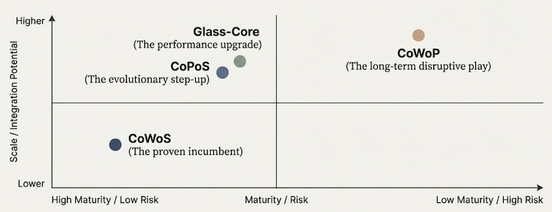
Figure 4. CoWoP may be the leading technology for advanced packaging in the future. For now, it presents a high risk and little maturity for today’s packaging designers.
Choosing Paths, Not a Single Winner
Given these diverging options, it is tempting to ask which one will “win.” A more realistic view is that all four will coexist, each serving different parts of the market:
- CoWoS remains the default for flagship AI accelerators and high-end networking ASICs whenever schedule and technical risk must be minimized.
- CoPoS becomes attractive for ultra-large, high-bandwidth packages when panel-level flows are proven in production and capacity is in place.
- Glass-core panels act as an upgrade path for substrates, either complementing or partially replacing silicon interposers in select applications.
- CoWoP may eventually provide a simplified, cost-efficient path for volume systems once ultra-HDI PCB manufacturing and inspection are mature.
Most companies will not bet everything on a single branch. Instead, they will segment their portfolios:
- The top of the product stack stays on CoWoS until panel-level alternatives are clearly ready.
- Mid-range accelerators and specialized data center chips migrate earlier to CoPoS or glass-core substrates, where package cost is more critical than absolute interconnect density.
- Edge AI, consumer, and automotive products explore CoWoP-like flows once the board ecosystem can support them, taking advantage of more straightforward assembly and thinner stacks.
Practical Guidance for Design Teams
While the ecosystem evolves, architects and physical designers can reduce future pain with a few pragmatic steps:
- Keep interfaces packaging-aware, but not packaging-locked: Floor plans, bump maps, and interface pitches should be designed to support both interposer-based and panel-level substrates without requiring complete rework. Avoid assumptions that only make sense in a single process.
- Simulate multiple stacks early: CoWoS, CoPoS, glass-core, and CoWoP each change the thermal path, mechanical behavior, and power-delivery network. Running system-level analysis for several candidate stacks can reveal which options are viable and where the real bottlenecks are likely to be—before package selection is frozen.
- Cultivate relationships across the supply chain: Foundries, OSATs, substrate makers, panel houses, and PCB vendors will not all move at the same pace. Access to capacity and early information will often matter more than the logo on a roadmap slide. A broad network of partners gives design teams more room to maneuver as technology and demand evolve.
Advanced packaging is no longer just a back-end detail: it is a central part of system architecture, cost structure, and time-to-market. The good news is that we are getting more options, not fewer. If we design with those options in mind—and keep our roadmaps flexible—the upcoming fork in the road can be an opportunity to differentiate rather than a constraint that slows innovation.
For teams initiating multi-die designs, Faraday offers fabless OSAT services that connect advanced packaging innovation with manufacturability, serving as a single partner from design through production. By managing a network of foundries, memory suppliers, packaging manufacturers, and testing partners,
Faraday addresses challenges related to 2.5D and 3D integration. This includes signal and power integrity, thermal constraints, and reliability without requiring in-house expertise. This approach enables developers to differentiate their systems while leveraging expert OSAT capabilities, reducing risks associated with transitioning to packaged silicon, and accelerating time-to-market for advanced packaging projects.
All images used courtesy of Faraday Technology.