Facebook
 Google
 GitHub
 Linkedin
GaN for AI Power Delivery: Performance, Integration, and Architecture
Learn how low-voltage GaN technology and integrated power architectures enable the high-density, highly efficient power delivery needed for next-generation multi-kilowatt AI processors.
Artificial intelligence is reshaping computing, but behind every new generation of GPU and accelerator lies a less visible challenge: how to deliver more power in less space, with higher efficiency and faster dynamic response.
As AI processors move from hundreds of watts toward multi-kilowatt power levels, conventional silicon-based power architectures are increasingly being pushed to their limits. This is driving a fundamental evolution in AI power conversion, from conventional low-frequency architectures toward high-frequency, high-density power systems.
Gallium nitride (GaN), particularly at low voltages, is emerging as an important technology for addressing these challenges. Low-voltage GaN power devices combine low on-resistance, fast switching and high power density, making them particularly relevant to the final stages of power delivery in AI systems. But the transition is not simply about replacing silicon with GaN. It requires advances in magnetics, capacitors, packaging, sensing, thermal management, and system architecture.
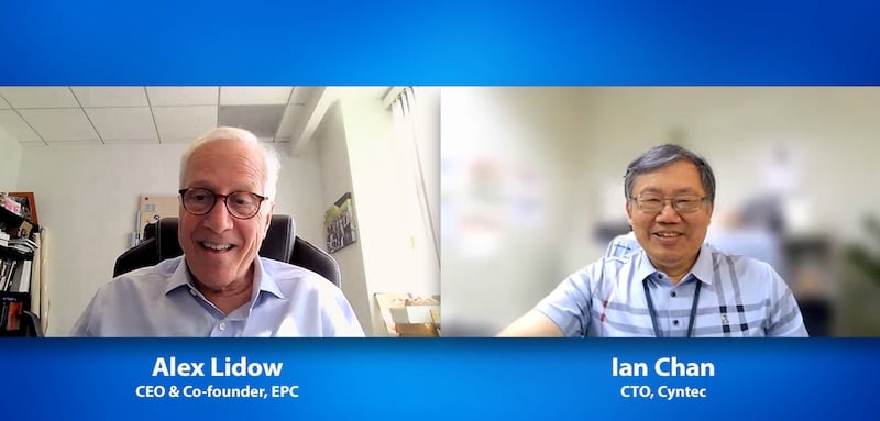
Alex Lidow and Ian Chen
As AI data centers move toward 800 VDC power distribution and increasingly distributed power conversion, the relationship between the GaN device and the rest of the power-conversion ecosystem becomes critical. The future of power electronics will increasingly depend on how these technologies work together.
From Low-Voltage GaN to High-Density AI Power
For many years, GaN power devices were primarily associated with applications where high switching frequency and efficiency could justify their additional cost and design complexity. That equation is changing rapidly, particularly at low voltages.
According to Alex Lidow, CEO and co-founder of EPC, the technology has reached an important point in its development: GaN transistors are now outperforming silicon MOSFETs across multiple performance metrics at voltage ratings of approximately 40 V and below. At the same time, manufacturing economics have improved sufficiently to open the technology to significantly larger application spaces.
“It’s really only in the last year that GaN transistors have surpassed MOSFETs at low voltages, say 40 volts and down, in terms of all performance metrics.”
This is particularly relevant because lower-voltage power conversion represents a very large portion of the overall power electronics market. As voltage decreases, current increases for a given power level, making conduction losses and power density increasingly important.
For AI data centers, this low-voltage domain is particularly important because the final power-conversion stages must deliver extremely high currents to GPUs and accelerators operating at very low voltages.
AI Infrastructure is Bringing This Challenge Into Sharp Focus
The power consumption of single AI processors has skyrocketed. “What we’re seeing is a shift from processors that draw a few hundred watts to devices that require two, even three kilowatts,” says Cyntec CTO Ian Chan. This leads to two concurrent design constraints: efficiency and physical space.
The power converter must manage huge currents in a smaller and smaller footprint. The higher the switching frequency, the more it can help by reducing the size of inductors, transformers, capacitors and other passive components. But higher frequency also spotlights the limitations of the rest of the power ecosystem.
“In the AI data center, each computing tray has a very limited footprint. GaN provides very good performance because you can operate at higher frequency, reduce the size and increase the power density needed to support the current."
Chan’s experience with GaN power modules provides a concrete example of how this translates into system-level design. In a 48 V-to-12 V power module targeting approximately 1 kW, he describes using four GaN devices compared with eight silicon superjunction MOSFETs. This reduction in device count contributed to a smaller module footprint and higher power density. He also points to the ability to operate above 1 MHz, compared with approximately 500–600 kHz for the silicon solution, creating further opportunities to reduce the size of magnetic and other passive components.
The result is a fundamental shift in power converter design. Semiconductor performance alone is no longer sufficient. A GaN transistor capable of operating at higher switching frequencies creates opportunities for smaller magnetic components, but those components must also operate efficiently at the same frequencies. Magnetics, capacitors, current sensing, gate drivers, controllers, layout and thermal management therefore become integral parts of the design.
This is where the relationship between EPC and Cyntec becomes particularly relevant. The two companies represent different parts of the same power-conversion ecosystem: GaN power devices on one side and high-frequency magnetic and passive technologies on the other.
GaN should therefore not be viewed simply as a drop-in replacement for silicon. Its value emerges when the higher switching capability and low losses of the device are used to optimize the complete converter, from the semiconductor and magnetics to the package and PCB layout. Engineers need to consider the entire power-conversion loop, including parasitic inductance, magnetic losses, gate drive and thermal paths, to fully exploit GaN’s capabilities.
For AI power systems, where increasing current and limited space are driving the demand for higher power density, this system-level approach becomes increasingly important.
From 800 VDC to the Chip: Integration Becomes the Next Frontier
The next major challenge is architectural.
AI data centers are moving toward 800 VDC power distribution as rack-level power continues to increase. Instead of delivering large currents at relatively low voltage over long distances, higher-voltage distribution can significantly reduce conduction losses and enable more efficient power delivery.
The move toward 800 VDC is therefore not simply a change in bus voltage. It represents a broader transformation of the AI data-center power architecture, with power conversion becoming increasingly distributed between the facility, the rack and the processor.
In this architecture, AC power can be converted to an 800 VDC bus close to the rack, while subsequent conversion stages step the voltage down toward the levels required by GPUs and other accelerators.
Lidow describes this as a separation of the power-delivery function into different physical locations. A sidecar can perform the initial conversion and establish the 800 VDC bus, while highly distributed conversion stages located closer to the load perform the final voltage transformation.
One architecture attracting attention is the use of input-series, output-parallel (ISOP) converters. By connecting lower-voltage DC-DC converter modules with their inputs in series and outputs in parallel, the architecture can handle the high input voltage while maintaining the advantages of low-voltage power stages.
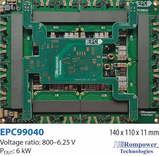
EPC99040 800 V to 6 V
“The 800-volt primary side is going to be done in a multi-stage ISOP topology. You can take low-voltage DC-DC converters, stack their inputs in series and their outputs in parallel, and get very high conversion efficiency,” says Lidow.
This architecture also illustrates why low-voltage GaN remains relevant even as the industry moves toward an 800 VDC bus. The high-voltage distribution layer and the low-voltage point-of-load stages solve different problems and can benefit from different semiconductor technologies.
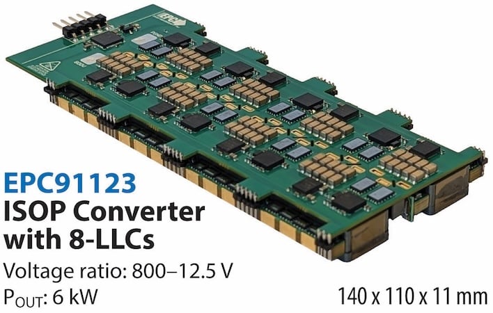
EPC91123 800 V to 12.5 V
The Challenge Then Moves From the Rack to the Processor
Modern GPUs and AI accelerators require very high currents at very low operating voltages. If you want to pass that current through the regular PCB traces, you will have some large losses in conduction and distribution. Therefore, the final power conversion stage is being pushed ever closer to the processor package.
According to Chan, this trend is also forcing a radical change in the mechanical dimensions of the power module. Cyntec customers are asking for converter structures that are only a few millimeters high, compared with approximately 9 mm in previous generations.
At these dimensions, the power converter may need to integrate inductors, capacitors, semiconductor devices, sensing elements, and other components within an extremely constrained vertical volume.
“We used to make the Z-axis nine millimeters high. Now we are asked by our customers to reduce it to three millimeters. Under three millimeters, we have to embed the capacitor, inductors, and the chip.”
This is not simply a packaging challenge. It is a system-level optimization problem.
The passive components must maintain acceptable losses at increasingly high frequencies. The semiconductor must combine very low RDS(on) with fast switching. The package must minimize parasitic inductance while controlling thermal paths. The converter must also respond rapidly to the extreme transient currents generated by AI processors.
At the point of load, these requirements converge: high-frequency switching, low conduction losses, low parasitics, high current capability, thermal performance and extremely fast transient response must all be addressed within the same physical structure.
Low-voltage GaN becomes particularly interesting in this context. Devices operating at voltages around 18 V can provide extremely low on-resistance, potentially below that of competing silicon MOSFET technologies in comparable applications. Combined with high switching frequency, and excellent overvoltage capability, this can reduce both conduction and switching losses while enabling smaller passive components.
But the real opportunity is not any individual specification. It is the interaction between semiconductor, magnetics, capacitors, packaging, sensing, control, and thermal design.
For power engineers, this means that the next generation of AI power conversion will increasingly require a co-design approach rather than an individual-component optimization approach.
This is why the next generation of AI power systems will increasingly be developed as integrated platforms rather than collections of discrete components.
The same principle will extend beyond data centers. AI-enabled robotics, humanoid systems, autonomous vehicles, drones, and other machines will demand high computing power while operating within tight constraints on weight, volume, efficiency, and thermal management.
Lidow sees AI as the immediate driver, followed by what he describes as “AI kinetics”—the physical world of machines that use AI to move, interact, and operate autonomously. GaN's combination of high frequency, low losses, and compact implementation could make it relevant across these emerging platforms.
The common denominator across these applications is power density. Whether the system is an AI accelerator, humanoid robot, drone or autonomous vehicle, designers increasingly need to deliver more electrical power from a smaller and lighter power-conversion system.
The broader lesson for power electronics engineers is that the traditional boundaries between semiconductor design, magnetics, packaging, and system architecture are becoming increasingly blurred.
Future Power Engineers Will Need to Understand All of Them
As Lidow puts it, modern magnetics could ultimately become one of the largest remaining opportunities for improving system efficiency. Chan reaches a similar conclusion from a different perspective: engineers need multidisciplinary knowledge spanning power devices, passive components, packaging, and system requirements.
The evolution of AI power infrastructure therefore represents more than a transition to higher voltage or higher power. It is a transition toward increasingly integrated power systems, where every component must be optimized as part of the whole.
GaN is an important enabler of this transition, particularly in low-voltage, high-frequency power conversion. But its full value emerges when the semiconductor is designed together with the magnetics, capacitors, packaging and control architecture.
As AI computing continues to push power requirements upward, the next competitive advantage in power electronics may not come from a single breakthrough component. It will come from the ability to integrate multiple technologies into a simpler, more efficient and higher-density power architecture.
GaN is an important enabler of that transition. But its real impact will come from what engineers build around it.
All images used courtesy of EPC.