Facebook
 Google
 GitHub
 Linkedin
Implementing a Binary Parity Generator and Checker with GreenPAK
This app note implements a binary parity generator and checker with two data input variants, a parallel data input, and a serial data input. It describes the implemented logic, GreenPAKs implementation, and the obtained results.
This app note implements a binary parity generator and checker with two data input variants, a parallel data input, and a serial data input. It describes the implemented logic, GreenPAKs implementation, and the obtained results.
Binary serial transmissions are among the most widely used techniques for sharing information between devices by using wired or unwired transmissions. Within these transmissions, data errors are one of the most important problems that must be analyzed to obtain a reliable communication system.
The parity generating/checking method is one of the most widely used error detection techniques for data transmission; a parity bit is appended to the transmitted data to make the binary data’s sum of 1s either even or odd. This bit is used to detect errors during the transmission of binary data.
The message containing the data bits, along with parity bit, is transmitted from transmitter node to receiver node. In the receiver node, the number of high bits in the message is counted. If this number doesn’t match with the parity bit transmitted it means there is an error in the received data.
There are several different brands of commercial IC’s (CD40101, 74HC/HCT280) that implement the parity generator/checker. Supplementing a Dialog GreenPAK design can positively affect the affordability, size, and modularity of the design. For example, the same general GreenPAK design can be used whether the intended I/O is active-high, active-low, or a mix.
In this application note, the digital logic required to implement an integrated parity generator/checker managed by control signals is implemented. To do this, the app note implements two variants of parity checking. The first variant has a parallel input so that the data bits to be verified are loaded simultaneously. The second variant implements a serial input, loading the data with an asynchronous serial data transmission. To do this, a serial-to-parallel conversion is implemented within the GreenPAK.
To implement the parallel input binary parity generator and checker an SLG46536V is used. To implement the serial input variant an SLG46620V is used.
Digital Communications and Parity Bit
In digital communications, a parity bit is a bit added to a binary stream to ensure that the total number of 1-valued bits is even or odd. This technique is a simple and widely used method for detecting errors. There are two types of parity bit methods, called even parity bit and odd parity bit.
The odd parity bit system consists of counting the occurrences of bits whose value is 1 in the data stream. If the number is even, the parity bit value is set to 1, so the total count of occurrences of high bits in the entire stream including the parity bit is odd. If the count of high bits is odd, the parity bit value is 0. An example is shown in Figure 1.

Figure 1. Odd parity binary system
The even parity bit method employs inverse logic. If the count of bits with a value of 1 is even in the data stream, the parity bit value is set to 0 making the total count of high bits in the entire stream including the parity an even number. If the count of bits with a value of 1 is odd, the parity bit is set to 1 so the entire stream has an even number of high bits.

Figure 2. System Diagram
To detect errors, a receiver must calculate the parity bit of the received binary data stream and compare it with the received parity bit. If parity bits are the same, an error is not detected. If they are different, an error is detected.
The parity bit is only useful for detecting errors. It cannot correct any errors, because it is not possible to determine which bit is incorrect within the stream. If a binary stream with errors is received, the receiver must discard it.
This makes the parity bit error method not suitable for high noise to signal ratio mediums because a successful transmission can take a long time. The advantage of this method is that it only needs a single bit to detect errors, which can increase the number of transmissions within a period.
As an example, an odd parity bit transmitter transmits the previously analyzed stream. If a bit of the stream is changed, the receiver obtains a different parity bit if it is compared with the transmitted one. This effect is shown in Figure 3.

Figure 3. Odd parity check of an erroneous stream
The parity bit is used in applications where a simple error detector is needed and the transmission can be repeated if an error occurs. The most important application is in serial data transmission. It is based on a common format of 7 or 8 data bits, an even parity bit, and one or two stop bits.
Other applications of parity bits are SCSI buses, PCI buses, and many microprocessor instruction caches. Because the L-cache data is just a copy of main memory, it can be disregarded and re-fetched if it is found to be corrupted.
Logic Implementation
One of the main advantages of the parity bit for error detection is the simplicity of its calculation. To obtain even parity it is necessary to only perform the Modulo-2 sum, or XOR, of the data bits in the binary stream to obtain the parity bit.
Once the even parity is obtained, the odd parity can be obtained as the inverse of the even one.
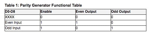
As stated before, this application note implements two variants of the binary parity generator and checker. Both have an even output bit and an odd output bit, which is set to a high level if the corresponding parity is detected. Also, they have an enable input. If the enable is high, the parity is calculated. Otherwise, both parity outputs are set to a low level.
In the parallel variant, the generator or checker obtains the parity bit of a 9-length binary stream. With this length, it can be used by the generator as a processor of 9 bits or as a processor of more than 9 bits by only using the MSB (the 9th bit) as the cascaded input of another processor.
In Figure 4, the logic diagram of the 9-bit length parallel input parity checker is shown.
.jpg)
Figure 4. Parity generator logic diagram.
Table 1 shows a functional table of the parity generator and checker.
In the serial variant, the input stage includes a serial to parallel conversion, so the output of the converter is connected to the parity generator circuit. This scheme is shown in Figure 5.
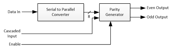
Figure 5. Serial input parity generator schematic diagram
This variant also includes an additional cascaded input, so more bits can be processed by using several 8-bit parity checkers.
Serial to parallel data conversion is based on Dialog’s AN-1120.
When there’s no data on the serial input pin the serial bus is held high. When a byte is going to be sent, a logic low start bit is sent before the byte to indicate a transmission. After that, the eight data bits are sent and finally, a stop high-level bit is sent. This sequence can be seen in Figure 6.

Figure 6. Serial data frame
Within several GreenPAK ICs the SPI block can be used to implement the serial-to-parallel conversion. The serial communication must have a 9600 baud rate.
A falling edge detection is implemented to detect the start bit. When it is detected, a connection flag bit is set so two counters/delays are triggered. One of them, titled Bit Timer, is configured to have a period equal to the bit time duration (1/9600). The other counter, titled Frame delay, is configured to have a delay time equal to the 10-bit frame period (10/9600).
With these timers, the SPI block is connected so that the serial data input pin is connected to the MOSI input and the Bit Timer output is connected to CLK. The eight data bits are received by the SPI block.
Additional logic is used for controlling the clock signal, so when the frame period has elapsed, the SPI clock stops and the data is held on the register.
More details of the SPI to Parallel converter can be found in Dialog’s AN-1120.
Implementation and Configuration
As described before, there are two variants of parity generator and checker, implemented with two different Dialog GreenPAKs.
The parallel input variant is implemented with SLG46536V.
To implement the bit inversion, as shown in Figure 4, 9 LUT’s were used, configured as inverters. This can be seen in Figure 7.
.jpg)
Figure 7. Bit inverter
The XOR is implemented to obtain the resulting bit for each nibble of data by using two 4-bit LUTs. They are configured as shown in Figure 8. As there aren’t more 2-bit LUTs available, the XOR between the two nibbles is processed with the 3-bit LUT3 with the third input connected to GND.
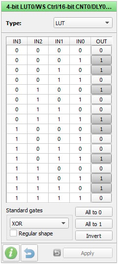
Figure 8. XOR processor
To obtain the resulting bits of processing the 9-th bit input, 3-bit LUT11 and 3-bit LUT12 are used by connecting input 2 to ground. They are configured as shown in Figure 9 and Figure 10 to process the XOR and XNOR respectively.
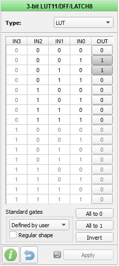
Figure 9. 9-th bit XOR
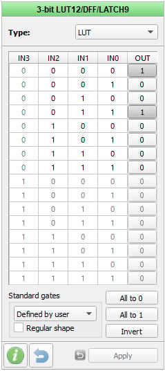
Figure 10. 9-th bit XNOR
Finally, the even bit and odd bit are individually AND’ed to the enable bit and VDD using 3-bit LUT14 and 3-bit LUT15 respectively. These configurations can be seen in Figure 11 and Figure 12.
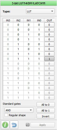
Figure 11. Even output control
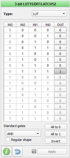
Figure 12. Odd output control
The entire parallel input parity generator and checker design is shown in Figure 13.
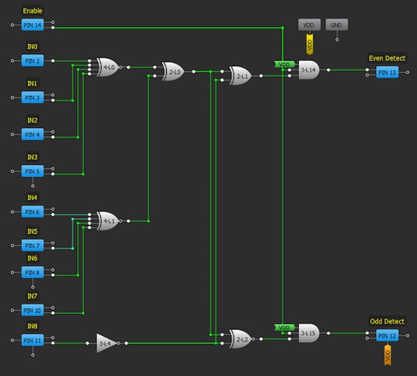
Figure 13. Parallel input parity generator and checker
The serial input variant is implemented with the SLG46536V. It has two matrixes that can be interconnected, so one of them was used to implement the serial-to-parallel converter and the other to implement the parity logic.
In Figure 14 and Figure 15, the Matrix 0 of the SLG46536V can be seen with the implemented serial-to-parallel converter.
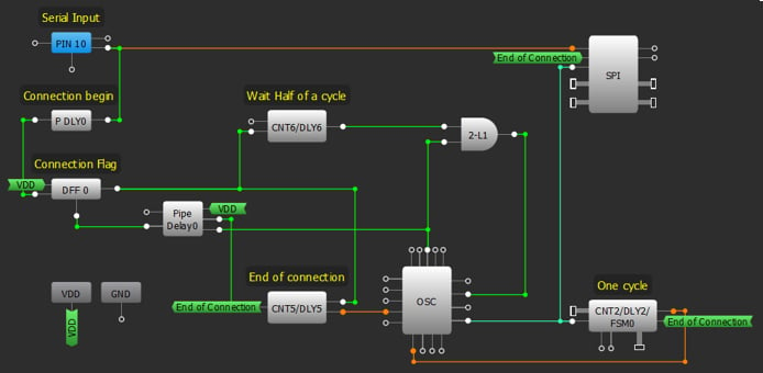
Figure 14. Serial-to-parallel converter (matrix 0)
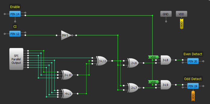
Figure 15. Serial-to-parallel converter (matrix 1)
Pin 10 is used as the serial data input. As mentioned before, a falling edge detector with a delayed output is implemented with P DLY0. This signal is used to indicate the start of reception, held by DFF0 and DLY6.
Once the transmission has started, CNT2 generates a signal with a frequency equal to 9600. This is done by dividing the output clock of the Oscillator, which corresponds to the internal Ring Oscillator controlled by the 2-bit L1. CNT2 configuration can be seen in Figure 16.
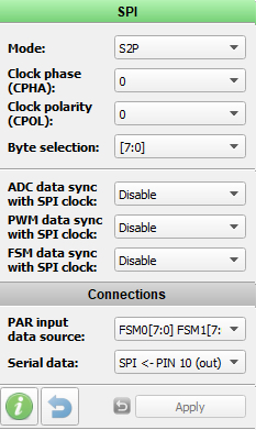
Figure 16. CNT2 configuration
The data is received by the SPI block, configured in S2P mode and with an 8-bit data length. This can be seen in Figure 17.

Figure 17. SPI configuration
The reception is enabled until CNT5 reaches the maximum count, which is configured to be 8/9600 to receive the eight data bits. The counter uses the internal RC oscillator (2 MHz) divided by 24. Its configuration can be seen in Figure 18.
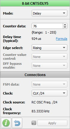
Figure 18. CNT5 configuration
Once the data is received, it is processed by the logic implemented in Matrix 1. Matrix 1 can be seen in Figure 19.
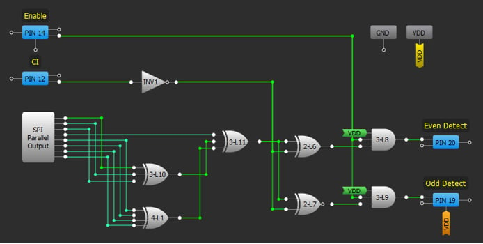
Figure 19. Serial input parity checker
Data bits are obtained from the parallel output of the SPI Module. The XOR of the eight bits is implemented with 3-bit LUT10, 4-bit LUT1, 2-bit LUT4 and 2-bit LUT5. Finally, 2-bit LUT6 and 2-bit LUT7 implement the XOR and XNOR with the cascaded input (Pin 12) respectively. The enable controls are AND’ed by 3-bit LUT8 and LUT9.
Results
To test the implementation, the two variants of binary parity generator and checker were analyzed separately.
The parallel input parity generator was tested by generating known data to be processed by the Generator so the output can be checked. In this case, the used data was
Data
0X1110011
X was a bit changing from 0 to 1 periodically. This way, an Odd result was expected when X is 0 and Even result was expected when X is 1.
The input signals and the Odd and Even Detect outputs where measured with a logic analyzer. In Figure 20, the logged signals are shown to behave correctly.
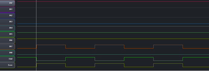
Figure 20. Parallel input parity generator test
The serial input parity generator variant was tested by independently transmitting two bytes, processing them, and verifying the result. The transmitted bytes were chosen to analyze an odd byte and an even byte.
In the odd data case, the used data was
Odd Data
11001101
In Figure 21, the serial input data and the Odd and Even detect Outputs, logged with a logic analyzer, are shown.

Figure 21. Serial input parity generator odd test
The odd output is low until the Odd data is received. After that, the Odd detect output is high and the Even detect output is low.
In the even data case, the used data was 10011001.
In Figure 22, the serial input data and the Odd and Even detect Outputs, logged with a logic analyzer, are shown.

Figure 22. Serial input parity generator even test
In this case, the previous odd data was re-sent so the Odd output is high, and the Even output is low prior to receiving the even data. After the even data is received, the Odd detect output is low and the Even detect output is high.
Conclusion
In this application note, we implemented two variants of a binary parity generator and Checker to be used as an error detection technique for data transmission. A parity bit is added to the transmitted data to make the number of 1s either even or odd. This bit is used to detect errors during the transmission of binary data. Several commercial IC’s can be replaced with Dialog GreenPAKs so that the application size and cost can be reduced. The two variants show how the data input method can be either parallel or serial. This is useful for applying the parity generator in different applications.
This article was co-authored by Alberto I. Leibovich and Pablo E. Leibovich.
References
For related documents and software, please visit:
https://www.dialog-semiconductor.com/configurable-mixed-signal.
Download our free GreenPAK Designer software [1] to open the .gp files [2] and view the proposed circuit design. Use the GreenPAK development tools [3] to freeze the design into your own customized IC in a matter of minutes. Dialog Semiconductor provides a complete library of application notes [4] featuring design examples as well as explanations of features and blocks within the Dialog IC.
- GreenPAK Designer Software, Software Download and User Guide
- AN-CM-xxx Binary Parity Generator and Checker.gp, GreenPAK Design File
- GreenPAK Development Tools, GreenPAK Development Tools Webpage
- GreenPAK Application Notes, GreenPAK Application Notes Webpage
- SLG46536V Datasheet (PDF)
- SLG46620V Datasheet (PDF)
- AN-1120 Bluetooth-Controlled Car/Robot, Application Note (can be downloaded from this page)
Related Content