Facebook
 Google
 GitHub
 Linkedin
Improper Power Sequencing in Op Amps: Analyzing the Risks
This article takes a look at the activity of op amps in different power sequence situations, analyzes possible issues, and presents some suggestions.
This article takes a look at the activity of op amps in different power sequence situations, analyzes possible issues, and presents some suggestions.
In systems with multiple supply voltages, operational amplifier power supplies must be established simultaneously with or before any input signals are applied. If this doesn’t happen, overvoltage and latch-up conditions can occur.
However, this can sometimes be a difficult requirement to meet in realworld applications. This article takes a look at the activity of op amps in different power sequence situations (see Table 2), analyzes possible issues, and presents some suggestions.
Power Sequencing Issues Can Vary
There are a number of different scenarios where power sequencing issues may arise. For example, in one customer application, an AD8616 can be configured as a buffer, the input is 0 V before power supplies are established (Figure 1), and the negative supply is powered on before the positive supply (negative power is present and positive power is absent).
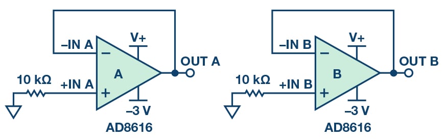
Figure 1. AD8616 test circuit with –3 V V– applied and V+ absent.
Table 1 shows the results of all AD8616 pins in such conditions. Before V+ is applied, the voltage at the V+ pin and OUT pins is negative. This may not damage the op amp, but if these signals are connected to terminals on other chips that haven’t been fully powered (for example, assuming the ADC uses the same V+, and its power pin normally tolerates only –0.3 V minimum voltage), the chips may suffer damage. A similar issue will happen if V+ is powered up before V–.
Table 1. AD8616 Pins’ Voltage with –3 V V– Applied and V+ Absent
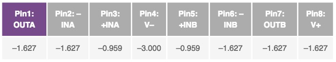
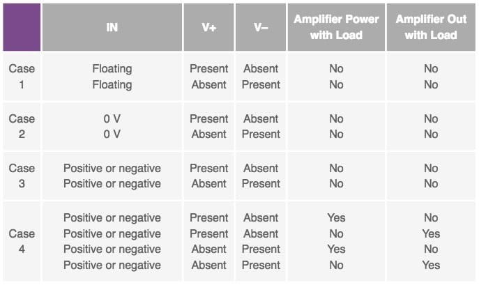
Table 2 highlights some possible situations in power sequencing.
Table 2. Possible Situations in Power Sequencing
Electrostatic Discharge (ESD) Diodes Within Op Amps
Electrostatic discharge can also result in an overvoltage event. Most op amps have an internal ESD diode to prevent electrostatic ESD events. ESD diodes can provide a key to analyzing activity when either V+ or V– is absent. Figure 2 is a simplified block diagram of the ADA4077/ADA4177. Table 3 shows the ADA4077-2/ADA4177-2’s typical drop voltage of internal ESD diodes and back-to-back diodes. Notice that back-to-back diodes are placed between the two input terminals of the op amps to clamp the maximum differential input signal.
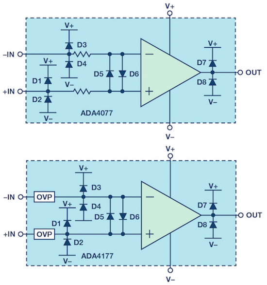
Figure 2. ADA4077/ADA4177 simplified block diagram.
Table 3. Internal Diode of an Op Amp
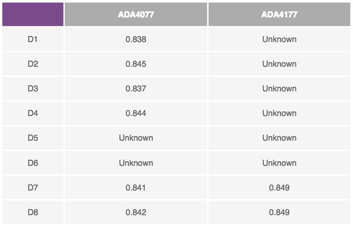
Also note that when DMM is used to measure D5/D6 of the ADA4077-2, it shows no diode between the two input terminals. In fact, there are two series of resistors before the back-to-back diodes to limit input current smaller than ±10 mA. The internal resistors and back-to-back diodes limit the differential input voltage to ±Vs to prevent a base-emitter junction breakdown.
For the ADA4177, OVP cells are integrated for robustness. They are placed before the ESD diodes and back-to-back diodes, so it’s hard to measure these diodes by DMM. The output ESD diodes of ADA4177 can be measured.
Evaluation Setup
Figure 3 is used to measure the activity of the op amp. Channel A and Channel B are each configured as a buffer, and the Channel B noninverting input is connected to the GND by a 100 kΩ resistor. By making V+ absent (V– present) or V+ present (V– absent), the input and power-related variables can be measured by the ampere and voltage meters. “By analyzing these variables, we can determine the current flow path.
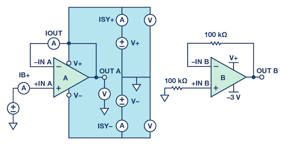
Figure 3. Setup for power sequencing test.
Case 1: Input Is Floating
Table 4 shows the results of a floating input and one absent supply. When V– is present and V+ is absent, there is a negative voltage at the V+ pin. When V+ is present and V– is absent, there is a positive voltage at the V– pin.
Testing the ADA4077-2 and ADA4177-2 reveals similar results. No large currents are observed at the input pins and power pins, and the op amp with floating input remains safe when a power rail is absent.
Case 2: Input Is Grounded
Table 5 shows the results when the input is grounded. Note for IB+, a negative value means the current flow out of the +IN terminal. For IOUT, a negative value means the current flow out of the –IN terminal.
Table 4. ADA4077-2/ADA4177-2 Results with Floating Input
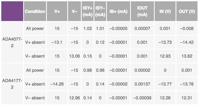
Table 5. ADA4077-2/ADA4177-2 Results with Grounded Input
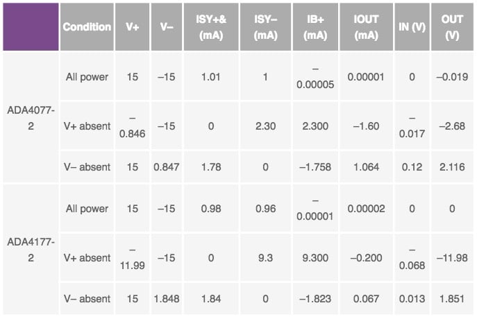
Taking ADA4077-2 with V+ absent as an example, V+ is clamped to the VIN voltage by an ESD diode.
- VIN is connected to V+ via an ESD clamp diode, so when VIN is 0 V, V+ is –0.846 V.
- Current flow path loop: as the red path shown in Figure 4, 0.7 mA current flows from GND (+IN) to V+. 1.6 mA current flows from GND (+IN) through an internal resistor, D5 and the feedback path between –IN and OUT, then the current flow into output terminal. Finally the two currents (0.7 mA and 1.6 mA) combine to flow to –15 V, and the combined current flows back to GND (+IN).
Results are similar between the ADA4177-2 and ADA4077-2. Note that within the ADA4177-2, D1 is implemented by an emitter base of a lateral PNP transistor. The transistor routes the overvoltage current away from the V+ to the V–. The ADA4177 circuit in Figure 4 shows 9.1 mA current flow from V+ back to V– , and combined with 0.2 mA current in the feedback path, results in a 9.3 mA current flow to –15 V, then the current flows back to GND.
No large currents are observed at the input pins and power pins for either the ADA4077-2 or the ADA4177-2 (Table 5). These op amps can withstand any order of PU sequencings in a gain of +1 with +IN grounded.
Case 3: With Input
A positive or negative signal (+10 V or –10 V) is applied to the +IN terminal when one power is absent. Table 6 shows no large current, so these op amps can withstand any order of PU sequencings in a gain of +1 with +IN grounded for a short duration.
The current flow path analysis is similar with Case 2 (0 V input), refer to Figure 5.
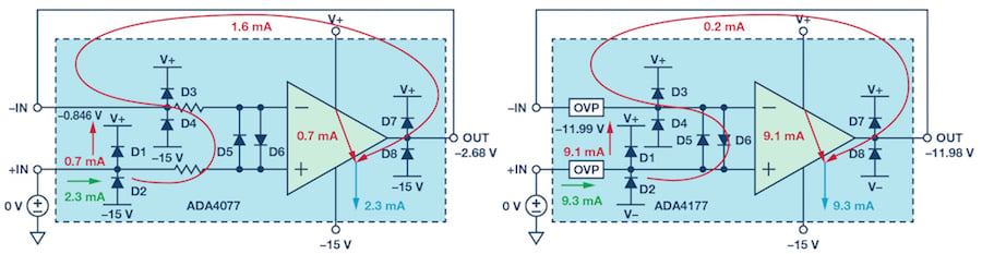
Figure 4. ADA4077/ADA4177 current path when V+ is absent (input grounded).
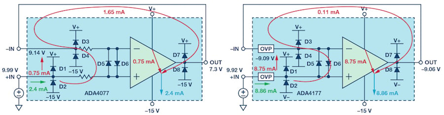
Figure 5. ADA4077/ADA4177 current path when V+ is absent (10 V input).
Table 6
Case 4: With Input and with Load at Power/Output
In a real application, the op amp circuit may work with another circuit. For example, the op amp’s output may drive a load, or the op amp’s power supply may also power other circuits. This can cause a problem.
In this test, a 47 Ω resistor is connected between the output and GND or the absent power pins and GND. Table 7 shows the test results for the ADA4077. Large currents are highlighted in red. Three possible situations can pose risks, assuming V+ is absent:
Situation 1: When the input is 10 V and the load of OUT is 47 Ω, the output is 1.373 V. When there is a 23 mA current flow out of the op amp’s output pin (refer to Figure 6) the current path is:
- Input signal source supply 30.2 mA current
- 24 mA current flow through D1 to V+, and 6.2 mA current flow through D5 and feedback path to OUT
- 24 mA current from V+ is divided to 1 mA (to V–) and 23 mA (to OUT)
- 29.2 mA current flow through 47 Ω load to GND
The current needs to be limited. By adding a 1 kΩ resistor at +IN, the input current is decreased to 6.8 mA.
Situation 2: When the input is 10 V and the load of V+ is 47 Ω, 170 mA current flows into the ADA4077-2 and flows out of V+ pin to a 47 Ω power load. 170 mA current will burn the internal diode and damage the chip. By adding a 1 kΩ resistor at +IN, the input current is decreased to 8.9 mA. Figure 7 shows the current flow path.
Table 7. ADA4077 with Load at Output Pin or Absent Power Pin
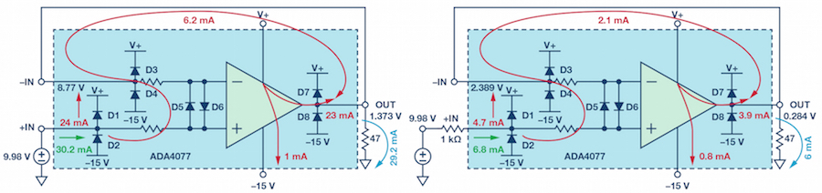
Figure 6. ADA4077 current path when V+ is absent (10 V input and 47 Ω output load).
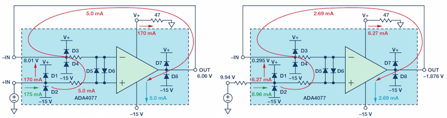
Figure 7. ADA4077 current path when V+ is absent (10 V Input and 47 Ω power load).
Situation 3: When input is negative (–10 V) and the load of OUT is 47 Ω (refer to Figure 8), there is a 48 mA current that flows through the chip. This will generate a 48 mA × (–2.5 V + 15 V) = 0.6 W power dissipation. Considering the ADA4077-2’s 158° C/W θJA , the junction temperature is 94.8° higher than the ambient temperature. If there are two channels or there is a heavier load, the junction temperature may be higher than 150°, and the chip may be damaged.
Instead of adding a current-limiting resistor at the input, the resistor should be added at the output.
When V+ is present and V– is absent, the same phenomena will happen. By adding external resistors to limit the current, the circuit can be more robust.
For ADA4177-2, only Situation 3 applies. When there is a large negative input and a heavy load at the output at the same time and when V+ is absent and there is 53 mA current flow through the chip, the power dissipation may be increased and the junction temperature is increased (refer to Figure 9). By adding a 1 kΩ resistor at the output, the risk can be avoided.
Of the two op amps, the ADA4177-2 is more robust than the ADA4077-2. It is a preferred choice for applications that require both precision and robustness.
Other Op Amp Activity in Power Sequencing
Among op amps, there are varying implementations of diodes, resistors, and OVP cells. Some op amps have no internal OVP cells, some have no back-to-back diodes. A different implementation will produce different results if one power supply is absent. In addition, different op amp designs can produce different results.
For example, the ADA4084-2 has no internal current-limiting resistor or OVP cells, and it has ESD diodes connected to the power supply and back-to-back diodes. Table 9 and Figure 10 show the results when V+ is absent and there is 10 V input. The ADA4084’s activity and current path are similar to those of the ADA4077-2 and ADA4177-2 (discussed previously in Case 3). However, because the ADA4084 has no internal resistor or OVP cell to limit the current, 60 mA current will flow into the chip, which may cause damage.
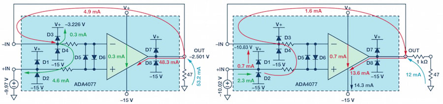
Figure 8. ADA4077 current path when V+ is absent (–10 V Input and 47 Ω output load).
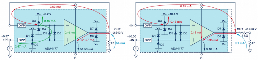
Figure 9. ADA4177 current path when V+ is absent (–10 V Input and 47 Ω output load).
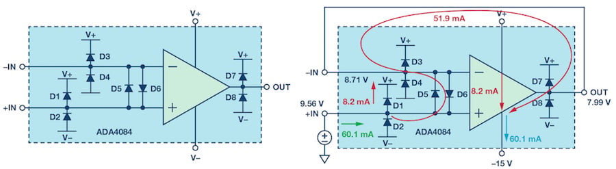
Figure 10. ADA4084 current path when V+ is absent (10 V input).
Table 8. ADA4177 with Load at Output Pin or Absent Power Pin
Table 9
In system applications, different op amps, different topology (such as noninverting amplification, inverting amplification, and difference amplification), different load, and external connections can be implemented. If one power supply is absent, the risks need to be evaluated. This article can provide guidance on setting up the evaluation circuit (Figure 2), how to analyze the current path, and evaluate the potential risks.
Summary
To avoid overvoltage or latch-up situations, operational amplifier power supplies must be established simultaneously. General guidelines are:
- During the Power On sequence, turn on the supply first, then apply a signal at the input
- During the Power Off, turn off the input signal first, then turn off the power supply
In real-world applications, these guidelines may be difficult to adhere to. This can cause problems, especially when there is an input signal, and designers need to properly evaluate the risk. An effective solution is try to limit the input current of the op amp so it is within the spec in the data sheet. Adding a current-limiting resistor at the input and output can help in applications where power can’t be supplied at the same time.
We tested three ADI op amps in a power supply absent application (ADA4084-2, ADA4077-2, and ADA4177-2). When integrated with internal resistors, the ADA4077-2 proved to be very robust. The ADA4177, when integrated with an OVP circuit, delivered the best robustness. In applications where the power may be absent, and external current-limiting resistors can’t be added, the ADA4177 is recommended to avoid degrading the precision.
References
ADA4077. Analog Devices, Inc.
ADA4177. Analog Devices, Inc.
Arkin, Michael and Eric Modica. “Robust Amplifiers Provide Integrated Overvoltage Protection.” Analog Dialogue, Volume 46, Number 1, 2012.
Blanchard, Paul and Brian Pelletier. “Using ESD Diodes as Voltage Clamps.” Analog Dialogue, Volume 49, Number 10, 2015.
For more information on the ADA4177 and ADA4077, see the product pages and data sheets here: ADA4177 and ADA4077.
Further Reading
This article was originally published by Analog Dialogue. Visit their website to view more technical articles.
Related Content