Facebook
 Google
 GitHub
 Linkedin
3 Pocket-Sized Photonics Innovations Power MedTech to Atomic Clocks
Research teams at EPFL, Harvard, and UC San Diego each reported photonic devices that shrink or repurpose light-based hardware.
Photonics keeps on absorbing and miniaturizing functions that once demanded a bulky optical bench. In the last few weeks, we’ve seen three research groups publish results that move light-based hardware toward smaller and more capable forms.
These teams have reported an ultrafast laser built onto a chip, a powerful on-chip ultraviolet source, and an optical device that hides and reveals images using humidity. Each leans on a core strength of photonics: precise control of light at a very small scale.
EPFL Folds an Ultrafast Laser Onto a Chip
Ultrafast, or femtosecond, lasers underpin spectroscopy, metrology, and optical atomic clocks, but the high-pulse-energy versions have stayed tied to table-top fiber systems. There’s historically been a research gap between integration and the ability to maintain pulse energy—something integrated photonics has spent the last two decades trying to close—with earlier on-chip lasers falling well short of fiber systems in pulse energy.
Now, EPFL researchers in Switzerland have reported the first integrated ultrafast laser that rivals those benchtop sources. The prototype is built on erbium-implanted silicon nitride photonic circuits with a Mamyshev oscillator, in which alternating spectral filtering and self-phase modulation produce mode locking.
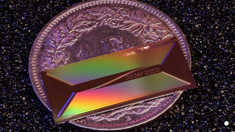
The photonic chip may replace much larger laboratory lasers, delivering short, high-energy optical pulses in a way that could revolutionize medical diagnostics and optical atomic clocks. Image used courtesy of EPFL
It delivers 1.05-nanojoule pulses as short as 147 femtoseconds, and its 42-cm cavity folds into a footprint the size of a match head. Because the chips can be manufactured at wafer scale, much like computer chips, the team estimates more than 1,000 cavities could be made at once, a route toward far cheaper ultrafast lasers. The group sees uses in spectroscopy, pollutant and defect detection, medical diagnostics, and compact optical atomic clocks for future communication and navigation, applications that have been held back by the cost and size of benchtop femtosecond systems.
Harvard Generates Usable UV On Lithium Niobate
Compact UV sources would benefit trapped-ion quantum computers, atomic clocks, and gas sensors. However, UV light attenuates rapidly in on-chip waveguides, which has long since limited the output to tens of microwatts. Now, a team from the lab of Marko Lončar at Harvard has closed that gap by generating UV light inside the chip rather than guiding it in, combining two red photons into one higher-energy photon.
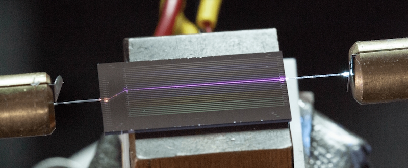
Harvard's chip-scale lithium niobate UV light source creates 120x more power than previous methods. Image used courtesy of Harvard
The Harvard researchers use a fabrication method they call “sidewall poling,” placing patterned electrodes along the sides of a thin-film lithium niobate waveguide to flip crystal domains with roughly 50-nm accuracy. Earlier approaches forced a tradeoff, since poling the whole film before etching limited later fabrication fixes, while poling after etching left the electrodes too far from the light to convert it efficiently.
The device produced 4.2 mW of on-chip UV at 390 nm, about 120x more than earlier thin-film lithium niobate demonstrations. That power level is very important for trapped-ion quantum computers, where key atomic transitions occur in the near-UV, and for compact sensors that track greenhouse gases and other pollutants.
UC San Diego Stores Hidden Images Using Humidity
Engineers at UC San Diego have built an optical device that displays different images depending on the moisture in the air, pointing toward reconfigurable storage and anti-counterfeiting labels.
The device uses a bilayer of antimony trisulfide beneath a grafted carboxymethyl cellulose hydrogel. As humidity rises, the hydrogel swells, changing the spacing between the layers and altering how light reflects, thereby swapping one hidden image for another.
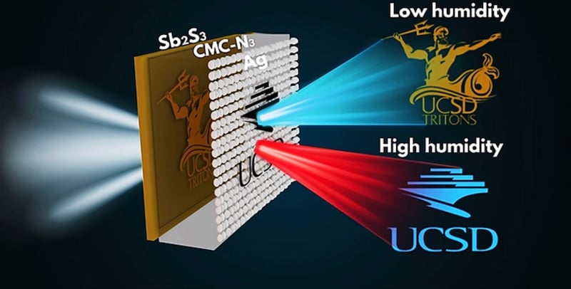
The optical device's bottom layer is made of antimony trisulfide, and the top layer is azido-grafted carboxymethyl cellulose. At low humidity levels, the UCSD Tritons logo appears, while the UCSD library logo appears at high humidity levels. Image used courtesy of UCSD
To demonstrate their work, the team showed a UC San Diego Triton logo giving way to a library logo. Transitions occur within 300 milliseconds, are repeatable, and can be set off by a person's breath. Beyond secure labels, the team points to interactive displays and environmental sensors that react to ambient moisture.
Reshaping Benchtop-Bound Photonics
The three results approach photonics from different directions, yet each replaces something larger or fixed with something smaller or reconfigurable: a benchtop laser, a bulky UV source, and static printed information. All three remain laboratory demonstrations, but each reports the kind of measured performance—from pulse energy to output power to switching speed—that engineers can design against.