Facebook
 Google
 GitHub
 Linkedin
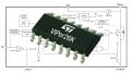
A New Line of Fast-Recovery Power MOSFETs from STMicroelectronics
These superjunction devices are rated for a drain–source voltage of 600 V and target high-performance switching applications.
These superjunction devices are rated for a drain–source voltage of 600 V and target high-performance switching applications.
My initial reaction to the MDmesh DM6 family from STMicro is a mixture of interest and concern: interest, because these FETs seem to offer an impressive array of features and capabilities; concern, because the complicated terminology in the press release makes me feel like I’m in a senior-year semiconductor class taking a test for which I’m not adequately prepared.
The MDmesh DM6 MOSFETs are fast-recovery, superjunction devices that have high dV/dt capability and improved on-state resistance compared to devices in the “previous generation” (I think that this refers to the M6 series, whereas the new devices are in the DM6 series).
Let’s see if we can unpack some of this information.
What Is a Superjunction MOSFET?
If you really want to dive into the world of superjunction technology, I recommend this app note from Vishay. If you are just looking for some basic information, read on.
The typical side-view depiction of a MOSFET that you’ve probably seen in textbooks corresponds to a “planar” MOSFET. The structure of a superjunction MOSFET is quite different. Instead of an individual doped area underneath the source and drain terminals, a superjunction MOSFET has a doped “column.” The following diagram conveys the difference between the two designs.

These diagrams were taken from an application note published by Vishay Siliconix. As you may have guessed, Vishay also sells superjunction FETs.
Despite the fact that the physical configuration of a MOSFET is typically depicted according to the planar structure, superjunction devices are widely used in high-power switching applications because they offer lower on-state resistance and reduced gate charge.
How Can a MOSFET Be “Fast-Recovery”?
If you think that recovery characteristics are typically associated with diodes rather than FETs, you are right, and in fact the DM6 series is described as fast-recovery because the devices include a fast-recovery diode.

Diagram taken from the datasheet for one of the DM6 devices.
My understanding is that as a general rule, you cannot rely on a MOSFET’s internal diode to suppress inductive kickback. However, in the case of the DM6 devices, STMicro expects that the body diode will be used for this purpose.
Recovery Time
In addition to fulfilling the typical requirements for a freewheeling diode in inductive switching applications, the DM6 body diode is intended to enhance the efficiency of the overall circuit.

Diagram taken from the DM6 product page. TRR is the reverse-recovery time, and Qrr is the reverse-recovery charge.
Ideal diodes conduct current in only one direction, but real diodes have something called reverse recovery. You can read more about reverse recovery in this article. The bottom line is that when a switching event occurs, the current flowing through the diode doesn’t decrease to exactly zero amps and then stay at zero amps. Rather, it overshoots into the negative region before settling into a zero-current condition.
This reverse current flows every time the circuit switches, and if the system requires frequent switching, all this reverse recovery will add up to a nontrivial amount of wasted power. Thus, to increase the efficiency of the circuit, we can use a freewheeling diode with lower reverse-recovery charge (as shown in the diagram).
Zener Protection
You may have noticed something unusual in the component diagram shown above. In addition to the MOSFET itself and the body diode, the device has back-to-back Zener diodes between the gate and the source.
Actually, I’m not sure how unusual this is in the context of high-performance power MOSFETs, but in my low-voltage world I certainly don’t expect to see Zener diodes included in a MOSFET package. These integrated Zener diodes provide protection against ESD strikes and voltage transients. You could accomplish the same thing with external components, but this saves you a bit of design work.
The Dangers of Changing Voltage
STMicro describes the DM6 devices as having “extremely high dV/dt ruggedness.” The term dV/dt is a calculus-notation-based abbreviation for the change in voltage with respect to time. More specifically, it refers to the change in a MOSFET’s drain–source voltage with respect to time.
If the rate of change of the drain–source voltage exceeds the device’s capabilities, the MOSFET may actually start to conduct (i.e., when it’s not supposed to). This is bad in itself, and the situation can lead to a serious failure. The two DM6 devices that I checked had a dV/dt ruggedness rating of 100 V per nanosecond. This seems pretty good, but honestly I don’t spend much time looking at power MOSFET datasheets, so I’m not sure how this number compares to the newest devices from other manufacturers.
If you have extensive experience with high-power switching applications, it’d be great to hear your insights regarding which MOSFET features are particularly valuable. You can share your thoughts in the comments section below.