Facebook
 Google
 GitHub
 Linkedin
Chiplet Summit 2025 Nods to a Bright Future for Disaggregated Computing
New solutions from big names like Arm and Keysight and up-and-comers like Numem were telling highlights from this year’s conference.
At the Chiplet Summit 2025, the industry’s best and brightest were out to display their latest advances in chiplet technology.

The Chiplet Summit was held at the Santa Clara Convention Center. Image (modified) used courtesy of the Chiplet Summit
So far this year, three major announcements have stood out to us, including news from Arm, Numem, and Keysight. Read on to learn these three newsworthy stories.
Arm's Chiplet System Architecture (CSA)
At this year’s Chiplet Summit, Arm announced that the first public specification of the Arm Chiplet System Architecture (CSA) is now available. Arm says that representatives from over 60 companies are now engaged with the CSA. These companies include ADTechnology, AMI, Alphawave Semi, Cadence, Jaguar Micro, Kalray, Rebellions, Siemens, Synopsys, and others.
The CSA supports modularity by defining distinct chiplet types, such as compute and I/O chiplets, which interact through standardized interfaces. Each chiplet type incorporates distinct properties and interfaces. For instance, compute chiplets facilitate high-performance processing through integrated Arm Processing Elements (PEs), while I/O chiplets carry out peripheral connectivity and interaction with external devices.
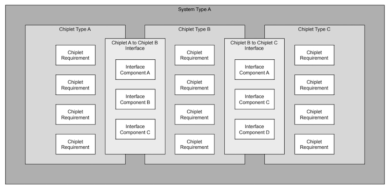
CSA component relationship. Image used courtesy of Arm
One goal of the architecture is to optimize designs for manufacturability by addressing yield improvements, cost efficiency, and technology reuse. To this end, protocol compliance is a central part of CSA implementations. The specification aligns with existing standards such as PCIe and Compute Express Link (CXL) for communication and memory coherence. It also provides guidelines for debugging and tracing through dedicated interfaces.
Further, the standard outlines specific interface classifications, including coherent and non-coherent memory traffic, interrupt handling, and system control communication. It also prioritizes flexibility by supporting chiplets with multi-role classifications so designers can leverage additional functionality across varied applications.
Numem’s NuRAM and SmartMem
At the Summit, memory provider Numem announced developments built on its patented NuRAM (MRAM-based) and SmartMem technologies.
Built on proven foundry MRAM processes, these solutions target HPC and AI workloads by combining nonvolatile memory with ultra-low power consumption and SRAM-like performance. The demonstrated memory subsystems offer 4-TB/s bandwidth per eight-die stack, a metric that surpasses existing solutions such as HBM4 and UCIe. Individually, each memory stack achieves capacities of up to 4 GB.
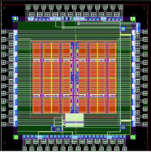
Numem’s test chip layout. Image used courtesy of Numem
Numem claims that its NuRAM technology reduces standby power by up to 100x compared to SRAM while delivering similar bandwidth. It is also said to achieve performance levels four to six times faster than HBM while operating with significantly lower power requirements. Further advanced features, such as in-compute intelligence, are said to enhance memory management through programmable power settings, self-testability, and optimized data processing.
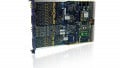
Keysight’s PHY Designer Chiplet Support
Keysight used the Summit to announce new features to its Chiplet PHY Designer 2025, enhancing high-speed digital chiplet design.

At the Chiplet Summit, Keysight's Chun-Ting "Tim" Wang Lee shows us the company's Chiplet PHY Designer.
The platform complies with UCIe 2.0 and Open Compute Project Bunch of Wires (BoW) standards to streamline pre-silicon validation for advanced 2.5D/3D or laminate package designs. The software advances simulation accuracy by including systematic signal integrity analysis and bit error rate (BER) assessment. The advanced clocking scheme analyses, such as the quarter-rate data rate (QDR) system, unlocks precise synchronization in high-speed interconnects.
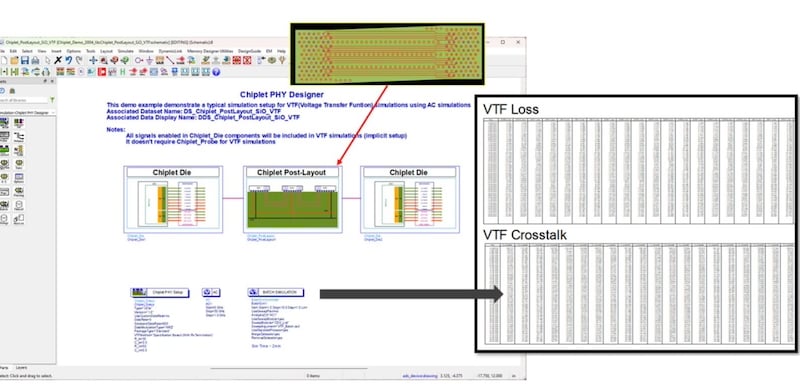
Chiplet PHY Designer workflow. Image used courtesy of Keysight Technologies
According to Keysight, the ultimate goal of Chiplet PHY Designer 2025 is to automate simulation workflows to reduce time-to-market by accelerating compliance testing, including voltage transfer function (VTF) evaluations.
Onward for Chiplets
The announcements from this year's Chiplet Summit reveal the momentum of disaggregated computing. As memory bandwidth demands continue to climb and traditional Moore's Law scaling faces mounting challenges, chiplet-based designs are becoming the norm in the industry. Now, a coordinated push toward standardization through initiatives like Arm's CSA and expanded UCIe support signals a maturing ecosystem. The real test will come as these technologies move from the lab to volume production.