Facebook
 Google
 GitHub
 Linkedin
Keysight Launches 3D Interconnect Designer for Chiplets and 3DICs
The W3510E workflow targets pre-layout modeling, EM analysis, and early UCIe and BoW validation for advanced AI infrastructure designs.
Keysight has introduced a new design workflow aimed at one of the more stubborn constraints in advanced packaging. The company positions its 3D Interconnect Designer, sold as the W3510E Chiplet 3D Interconnect Designer, as a pre-layout environment for defining, routing, and simulating 3D interconnect structures in chiplet and 3DIC packages.
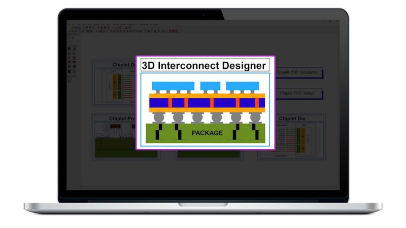
The W3510E Chiplet 3D Interconnect Designer is a pre-layout workflow for advanced multi-die integration, automated routing, simulation, and UCIe compliance.
The new tool extends Keysight’s digital design portfolio and works alongside its existing Chiplet PHY Designer. While the latter focuses on die-to-die link compliance and channel analysis, the 3D Interconnect Designer focuses on the physical construction of the interconnect itself, including silicon and organic interposers, microbumps, vias, bus interconnects, and patterned reference planes.
Moving Interconnect Decisions Upstream
As AI accelerators and high-bandwidth compute devices shift toward multi-die partitioning, the electrical performance of the package interconnect has become tightly coupled to overall system viability. Traditional flows often rely on iterative back-and-forth between layout and analysis tools, with detailed electromagnetic simulation occurring later in the process. That approach can expose issues only after substantial routing and integration work has been completed.
Keysight intends its 3D Interconnect Designer to shorten that cycle. The workflow allows engineers to define interposer structures, create breakout feeds for via arrays, and configure die-to-die bus connections before committing to a full package layout. The tool supports both component-level and interconnect-level simulation, enabling designers to evaluate electrical behavior at multiple levels of granularity.
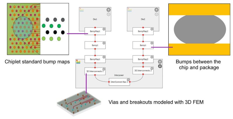
3D die-to-die interconnect modeling.
This pre-layout emphasis is critical in AI infrastructure projects, where a single iteration on a large silicon interposer can significantly delay schedules. By combining geometry definition with electromagnetic analysis within a single workflow, the company aims to reduce the manual iteration loop that has become a bottleneck in advanced package development.
Modeling Patterned Planes
One of the capabilities highlighted in the launch is support for patterned or “hatched” ground planes. These geometries, sometimes called waffled planes, are used in silicon interposers and bridges to improve manufacturability, control stress, or address material constraints. Unlike a solid reference plane, a patterned plane modifies current return paths and can alter effective impedance and coupling behavior.
In conventional modeling, such geometries can be abstracted or simplified to reduce computational burden. However, as data rates increase and die-to-die interfaces push tighter margins, those simplifications can mask second-order effects that become first-order problems at scale.

The W3510E Chiplet 3D Interconnect Designer enables users to quickly analyze data lines with hatched return planes.
The 3D Interconnect Designer supports rectangular and diamond hatch patterns in interposer definitions. By embedding these structures directly into the pre-layout workflow, engineers can evaluate their electrical impact without manually reconstructing geometry in a separate solver environment. That level of geometric fidelity can determine whether a channel meets its target without further redesign for advanced packages carrying wide die-to-die buses.
The tool’s focus on microbumps, via structures, and bus interconnects also reflects the practical realities of 2.5D and 3DIC packaging. These elements define parasitic inductance, capacitance, and coupling behavior as much as the PHY architecture does. Treating them as first-class design objects aligns the interconnect model more closely with physical implementation.
Early Validation Against UCIe and BoW
Beyond geometry and simulation, Keysight emphasizes early validation against emerging die-to-die standards, including UCIe and BoW. These standards define electrical and channel requirements for short-reach chiplet interconnects, with metrics such as voltage transfer function compliance forming part of the evaluation criteria.
Validating interconnect structures against these requirements before full-package layout reduces the risk of noncompliance being discovered late in the design cycle. In multi-die AI accelerators, where dozens of die-to-die links may share a single interposer, a late-stage channel failure can ripple across the entire integration plan.
By linking the 3D interconnect definition to standards-aware analysis, the workflow aims to align physical design choices with protocol-level constraints from the outset, something that will become particularly relevant as chiplet ecosystems mature and interoperability across vendors becomes more realistic.
All images used courtesy of Keysight Technologies.
Related Content