Facebook
 Google
 GitHub
 Linkedin
Memorable Memory: 5 Highlights From the Future of Memory & Storage Show
Industry leaders used FMS 2026 to introduce a suite of new memory advancements, from denser QLC NAND to 16,000 MT/s DDR5.
Last week was the Future of Memory and Storage (FMS) 2026 conference, and a handful of industry leaders used the show as a launching pad for new products. In this edition of Tech Shorts, we’ll look at five FMS announcements that address a different layer of the growing concerns surrounding memory for AI workloads.
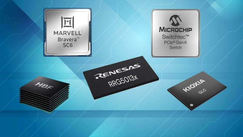
SK Hynix Unveils the First HBF Standard
To keep up with surging demand for memory and storage, many server designers have suggested adding a new high-performance memory tier between HBM and SSDs. SK Hynix and Sandisk laid the groundwork for one such new memory technology, High Bandwidth Flash (HBF), by releasing its first standard specification through the Open Compute Project (OCP).
In theory, HBF uses NAND to reach capacities HBM can’t, while still targeting HBM-class transfer speeds.
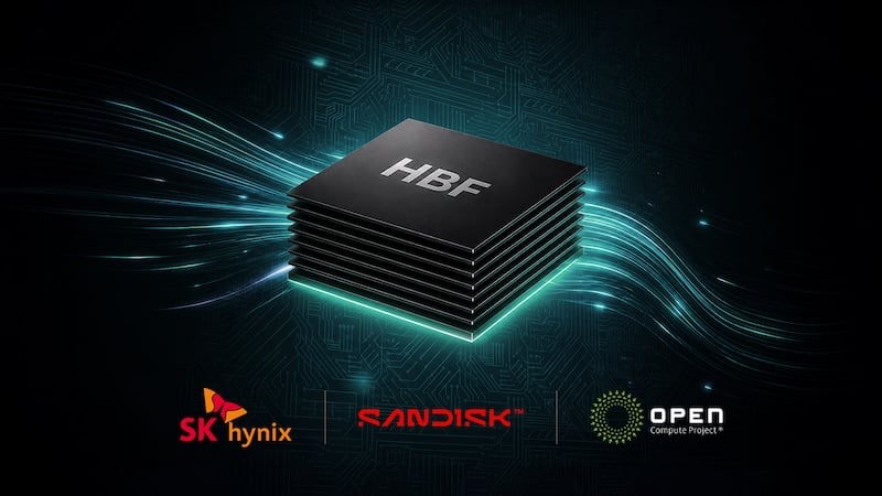
SK Hynix announced the first standard specification for High Bandwidth Flash (HBF) in collaboration with Sandisk through the OCP. Image used courtesy of SK Hynix
Per the specification, the two companies set HBF capacity at up to 512 GB from two stack configurations: an 8-high and a 16-high NAND die stack. They then sorted bandwidth into three grades spanning roughly 0.4 TB/s to 3.0 TB/s. For the processor connection, they adopted Universal Chiplet Interconnect Express (UCIe), which allows designers to attach HBF to GPUs and CPUs.
With Google and Tenstorrent joining the consortium, the HBF standard is well on its way to receiving mainstream industry adoption.
Kioxia and Sandisk Push QLC Bit Density Past 37 Gb/mm²
Today’s hyperscale storage buyers want more bits per die without sacrificing power efficiency or interface speed. To target this problem, Kioxia and Sandisk unveiled their tenth-generation quad-level-cell (QLC) 3D flash memory technology, which the companies say raises bit density by up to 60% over their eighth-generation devices and passes 37 Gb/mm². By reaching what they call “the industry benchmark for QLC bit density”, Kioxia and Sandisk significantly lowered the cost per bit for hyperscalers.
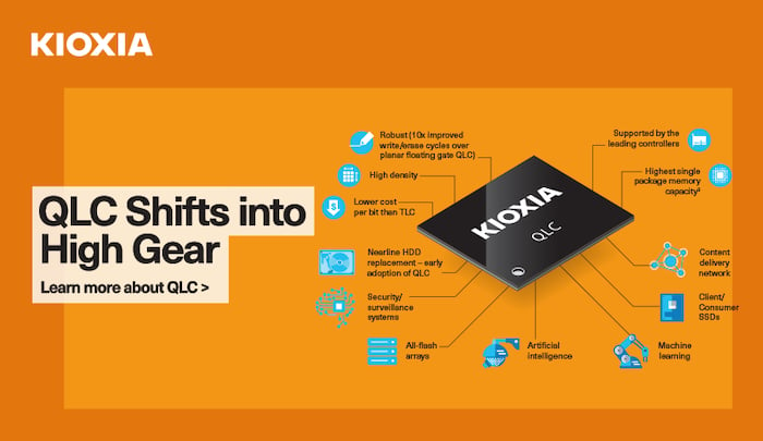
Kioxia’s QLC technology features. Image used courtesy of Kioxia
According to the companies, the gains are attributable to a new 332-layer architecture and a reworked floorplan. The memory solution is built on CMOS directly Bonded-to-Array (CBA) technology, where CMOS logic and memory arrays exist on separate wafers before bonding. That approach helped the design reach a 4.8 Gb/s NAND interface over Toggle DDR 6.0 and the Separate Command Address (SCA) protocol—a QLC first.
The pair also says a Power-Isolated Low-Tapped Termination (PI-LTT) scheme improves I/O data-out transfer power efficiency against the power and cooling limits of AI and cloud infrastructure.
Marvell Targets KV Cache Bottlenecks in AI Inference
A major problem in AI compute is minimal GPU utilization resulting from time spent waiting to fetch data from memory. To cut that waiting, Marvell announced several new products for its AI memory infrastructure portfolio, including spread-over-server storage, rack-scale memory pooling, and pod-level shared memory.
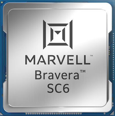
Marvell’s Bravera SC6 PCIe 6.0 SSD controller. Image used courtesy of Marvell
At the server level, the company says the new Bravera SC6 PCIe 6.0 SSD controller doubles the performance of its PCIe 5.0 Bravera SC5. Marvell built it to move more KV cache from high-bandwidth memory onto the SSD, which frees the scarcest memory in the server for active work.
Moving up to the rack, Marvell designed Structera X to let hyperscalers pool CXL memory and share it among servers. Bigger pools let one inference job draw on memory its own server does not have.
Finally, at the pod level, Marvell built an optical shared memory tier from Photonic Fabric modules, a NIC, and chiplets. That tier reaches accelerators in racks up to 50 meters away, and Marvell says it holds up to 32 TB of warm KV cache that reloads without a trip to storage. They claim the result is two to three times higher token throughput without increasing data center footprint or power usage.
Microchip and Micron Demonstrate End-to-End PCIe Gen 6 Storage
Recently, Microchip demonstrated an end-to-end PCIe Gen 6 storage architecture with Micron that pairs a Microchip Switchtec PCIe Gen 6 fanout switch with Micron 9650 NVMe SSDs. PCIe 6.0 doubles PCIe 5.0 bandwidth to 64 GT/s per lane, which Microchip says is only fully available to storage drives because of its newest switch.
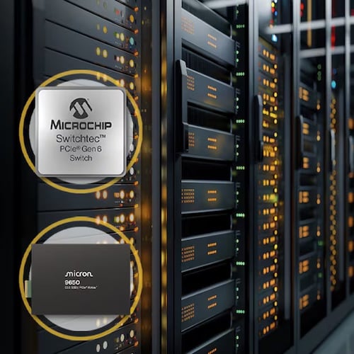
Microchip’s Switchtec PCIe Gen 6 switch paired with Micron’s 9650 NVMe SSDs in a data center. Image used courtesy of Microchip
Microchip builds the Switchtec Gen 6 switches on a 3-nm process and adds error containment, diagnostics, and multicast for one-to-many data distribution within a PCIe domain. For system integrity, the company added a hardware root of trust and secure-boot architecture backed by post-quantum-safe cryptographic algorithms that meet CNSA 2.0 security standards.
On the drive side of the link, Micron calls the 9650 the first mass-produced PCIe Gen 6 SSD. Microchip says the two parts support composable and disaggregated system designs, which lets data center architects scale storage separately from compute.
Renesas Raises MRDIMM Data Rates to 16,000 MT/s
Server architects who need more memory bandwidth typically don’t want to redesign their platform for it. For these customers, Renesas announced its third-generation DDR5 Multiplexed Rank Dual In-Line Memory Module (MRDIMM) chipset.
The company says the chipset reaches server-class speeds up to 16,000 MT/s and gives 25% higher memory bandwidth than the company’s second-generation solutions. Because Renesas reached the rate while keeping existing DDR5 infrastructure and standard DIMM form factors, server makers can easily boost their memory bandwidth without needing to redesign infrastructure.
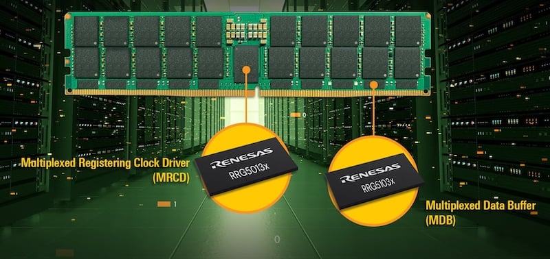
Renesas Gen 3 MRDIMM chipset enabled 16,000 MT/s. Image used courtesy of Renesas
Renesas built the chipset around a third-generation Multiplexed Registering Clock Driver (MRCD, RRG5013) and a Multiplexed Data Buffer (MDB, RRG5103). By surrounding them with power management ICs, Serial Presence Detect (SPD) hubs, and temperature sensors, the company hopes its MRDIMM chipset will be an all-in-one package for memory module manufacturers.