Facebook
 Google
 GitHub
 Linkedin
New Load Switch Underlines the Place of “True Reverse-current Blocking”
High-voltage electronics cause a number of issues for FETs used as load switches. A new device from Diodes Incorporated aims to tackle the long-standing issue of reverse current.
The growing need for high-voltage electronics (for instance, in data centers and EVs) has redefined what EEs need out of an integral component, the FET. For example, high-power applications have created a huge demand for FETs with the lowest possible RDS(on) to be used as load switches.
Lowering RDS(on) helps minimize power consumption in the form of IR losses—a fact that has spurred intense interest in wide-bandgap semiconductors.

Wide-bandgap semiconductors are being explored for high-power and high-frequency applications. Image used courtesy of Texas Instruments
Still, the problems don’t stop here. High-voltage electronics present another major challenge for FETs as load switches: reverse-current protection. Diodes Incorporated is looking to address this concern with its newest product: a p-channel power FET designed with “true reverse-current blocking."
Load Switches in High-voltage Electronics
In high-voltage applications, designers must find a way to save power in any way they can. One of the ways this is achieved is by implementing load switches into the circuitry.
Load switches are simply a means of connecting or disconnecting a load from a voltage rail as needed, making sure that no power is consumed by a load when not being used. This is typically implemented with one or two MOSFETs between a voltage rail and a load, controlled by an external logic signal.

Example of a load switch circuit. Image used courtesy of ON Semiconductor
In the example circuit above, the PMOS load switch is being biased by R1, such that when the enable signal is low, the PMOS is off, meaning that VIN and VOUT are isolated from one another. When the enable signal goes high, the gate of the PMOS is driven to ground, effectively connecting the load at VOUT to the voltage rail at VIN.
High Voltage Challenges
With an understanding of what these circuits look like, we can understand how high-voltage applications can create additional challenges.
Referring to the example circuit, as voltages (and subsequently currents) increase, the same pass FET will consume more power at the same RDS(on). This power challenge has inspired large investments into a new generation of FETs with lower on-channel resistance in order to decrease power consumption in these kinds of applications.

Reverse-current mechanism in a pass switch application. Image used courtesy of ROHM Semiconductor
Another challenge in high-voltage applications is reverse current. Due to the physical layout of a MOSFET, a parasitic diode exists between the device’s drain and source terminal. Hence, if VOUT ever gets larger than VIN, this parasitic diode becomes forward biased and causes a huge rush of current from VOUT to VIN known as reverse current.
Reverse current has become a greater concern in these applications since higher voltages lead to higher reverse currents, which could prove catastrophic to electrical systems.
Diodes Incorporated's Vision of True Reverse-Current Blocking
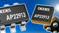
To address both of these issues, Diodes Incorporated has released a new product this week: a p-channel FET meant specifically for low-power pass switching applications.
The new FET, called the AP22916, features a decreased RDS(on) of 60 milliohms at 5 V, a quiescent current of 0.5 µA, as well as a feature called “true reverse-current blocking” (TRCB).

Functional block diagram of the AP22916. Image used courtesy of Diodes Incorporated
According to Toshiba, TRCB differs from conventional reverse current blocking because TRCB blocks the flow of reverse current when the load switch is enabled or disabled, whereas conventional techniques only protect when the load switch is disabled.
Diodes Incorporated claims this is implemented in its new switch by means of an internal reverse-voltage comparator, comparing VIN and VOUT at all times and allowing for “true” reverse-current blocking.
Finding a Place in Portable Applications
With an RDS(on) lower than previous solutions and TRCB built-in, the new product from Diodes Incorporated may be a useful solution to engineers designing in high-power fields.

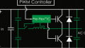
Typical application circuit for the AP22916. Image used courtesy of Diodes Incorporated
Packaged in a chip-scale house (0.78 mm x 0.78 mm x 0.45 mm), the AP22916 appears to offer high power density in portable applications ranging from mobile devices, wearables, and GPS devices, among others.
Featured image used courtesy of Diodes Incorporated