Facebook
 Google
 GitHub
 Linkedin
MIT Flips the Challenges of Chip Stacking On Its Head
Low-temperature BEOL transistors and memory elements aim to cut data-movement energy in AI workloads.
MIT researchers are pitching a new solution to one of modern computing’s most stubborn inefficiencies: the energy consumed by moving data between logic and memory. The team recently discovered that by adding additional active device layers to the back-end-of-line (BEOL) of a conventional CMOS chip, they could turn the region normally reserved for wiring into a stack that can host both logic and memory transistors.

The new technique stacks several active components on the back end of a computer chip to increase energy efficiency.
The researchers presented two related papers at IEEE IEDM, centered on BEOL indium oxide transistors and BEOL nanoscale ferroelectric memory devices.
A Bottleneck More Than Just Transistors
The starting point is the same architectural tax that keeps appearing in data center power budgets and edge devices alike. Since logic and memory are typically distinct structures, every compute step that depends on a stored state forces data to traverse interconnect and packaging boundaries.
That movement costs energy and time, and it becomes more punitive as workloads get more data-centric, including deep learning and computer vision pipelines. MIT frames the goal as reducing that shuttling by placing more functional elements closer together in a compact vertical stack.
3D stacking is not new, but monolithic stacking on top of finished logic is constrained by temperature. Standard silicon device fabrication often requires thermal budgets that can damage previously built transistors and metal layers. The MIT team’s core move is to avoid building new silicon devices “up front” and instead add active layers on the chip’s back end, where wires and metal bonds traditionally live.
That “flip” is important because it turns the BEOL into additional device real estate without asking the underlying CMOS to survive another high-temperature, front-end flow. It also shortens the physical path between compute, embedded memory, and interconnect, where energy is wasted in conventional layouts.
A BEOL Stacking Architecture
MIT’s proposed architecture is a vertically integrated device stack fabricated on the back end of an existing circuit, with added active transistor layers and memory elements formed above completed CMOS. The enabling device in the stack is a BEOL transistor with an amorphous indium oxide channel layer. Because of indium oxide’s properties, the team reports being able to “grow” an extremely thin layer at about 150°C, a temperature low enough to avoid harming the circuitry beneath it.
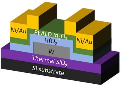
Schematic of the BEOL PEALD-In2O3-channel FET.
Materials control is the primary challenge in fabrication here. The indium oxide film is only about 2-nm thick in their process description, and its performance hinges on defect management. Oxygen vacancies help the channel conduct, but too many vacancies degrade switching behavior. The team says it optimized fabrication to minimize defects to the point that the resulting devices switch “rapidly and cleanly,” reducing the extra energy associated with turning transistors on and off.
In addition to logic-style BEOL devices, the researchers also demonstrated BEOL transistors with integrated memory by incorporating a ferroelectric hafnium-zirconium oxide (HZO) layer. This is a practical choice of material because hafnium-oxide-based ferroelectrics are already of interest for CMOS-compatible memory and computing concepts. The reported devices are on the order of 20 nm and achieved switching speeds of 10 nanoseconds, reaching the team’s measurement limits, while operating at lower voltage than comparable devices in the same class.
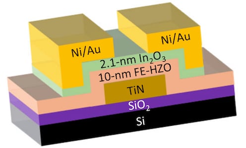
Schematic BEOL FE-FET structure.
The result is a stackable platform rather than a single device demo. One paper focuses on enhancement-mode BEOL indium oxide FETs and modeling, while the second targets ferroelectric switching dynamics in BEOL nanoscale ferroelectric field-effect transistors. MIT also notes collaboration with the University of Waterloo on performance modeling, a step that typically becomes important when moving from isolated devices to circuit-level integration.
Initial Applications
MIT’s work is not about replacing advanced-node silicon with oxide electronics, but rather about adding new functional layers where today’s chips mostly have routing. They then used that vertical integration to reduce the energy cost of data-centric computation. The most direct beneficiaries are workloads where memory traffic dominates, including AI inference, deep learning, and vision tasks that repeatedly stream activations and weights.
There is also an architectural angle because memory-capable transistors in the BEOL can enable tighter coupling between storage and compute for in-memory and near-memory compute schemes. Ferroelectric devices, in particular, are often discussed for dense nonvolatile storage and for analog or multi-level behaviors that can support neuromorphic-style operations. MIT emphasizes that shrinking the ferroelectric memory transistor down to nanoscale dimensions gives the team a platform to study the physics of individual ferroelectric units, which could influence how future memory and compute primitives are designed.
Near-term, the work reads as a tooling-and-materials milestone, with a low-temperature, defect-controlled path to place active transistors and memory elements on the back end of a finished chip without wrecking what is already there. MIT’s next stated step is to integrate BEOL memory transistors onto a single circuit and to push device performance while improving control over the ferroelectric layer’s properties.
All images used courtesy of MIT.