Facebook
 Google
 GitHub
 Linkedin
Paragraf Unwraps Graphene-Based FET Made at New Graphene Foundry
Paragraf recently introduced a new GFET, a next-generation graphene transistor platform designed for scalable molecular sensing and research applications.
Paragraf has introduced the PMF2000 GFET, a new graphene field-effect transistor platform designed for sensing and research applications that require greater consistency, repeatability, and scalable production. The device is the first product released from the company’s new large-wafer graphene foundry in Huntingdon, England, which Paragraf describes as the world’s first graphene foundry.
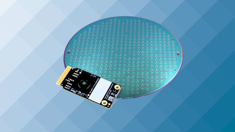
Paragraf's PMF2000 GFET.
The PMF2000 (datasheet linked) expands Paragraf’s GFET portfolio with a contamination-free, graphene-on-silicon device built using the company’s direct graphene growth process. The sensor targets molecular sensing applications in healthcare, agritech, chemical analysis, and industrial research. Paragraf hopes it will provide customers with a higher-volume production path without requiring changes to existing GFET-based designs.
Large-Wafer Manufacturing Targets Higher Consistency
Graphene devices have historically struggled with contamination, consistency, and scaling production beyond research-level volumes. Paragraf’s manufacturing process grows graphene directly on the substrate rather than transferring it via polymer-assisted methods, which helps reduce contamination and improve repeatability. With the PMF2000, the company is also giving existing GFET users a higher-volume production path without requiring major design changes.
Paragraf designed the PMF2000 as an electrolyte-gated field-effect transistor with three independent graphene sensing channels positioned around a central in-plane gate electrode. That layout creates a more uniform electric field during operation while also supporting multiplexed sensing and internal referencing.
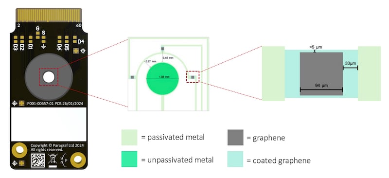
PMF2000 GFET sensor structure and channel layout.
The PMF2000 includes an epoxy encapsulation layer that helps simplify liquid handling and sensor modification during testing. Its three graphene channels can also be functionalized independently for multiplexed sensing or internal referencing. Paragraf designed the device to work with standard data acquisition systems through its plug-in GFET breakout platform, with typical operating conditions using gate voltages between +200 mV and +800 mV and source-drain voltages between 20 mV and 100 mV.
Built for Research and Molecular Detection Applications
The PMF2000 includes three graphene channels with a typical transconductance of 0.8 mS·sq/V and channel resistance ranging from 1 kΩ to 3.5 kΩ. The transistor uses platinum-based gate materials with 65-nm Al2O3 passivation and exposed platinum metallization. The maximum recommended operating voltages are ±1 V AC/DC, with operating currents up to 1 mA.
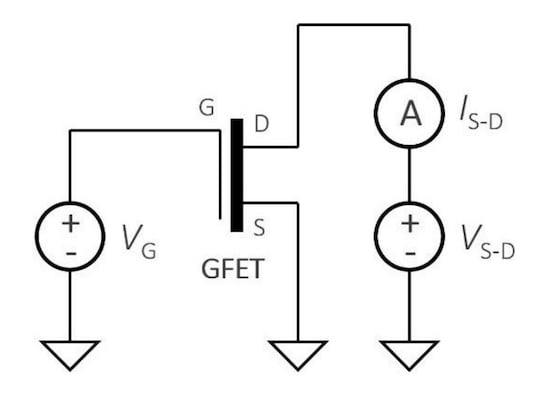
A basic electrical test circuit for the PMF2000 GFET.
Paragraf says it aims the PMF2000 at molecular sensing applications across healthcare, agritech, chemical analysis, and industrial research. The company is also positioning the platform as a way for customers to move from small-scale lab testing into higher-volume production without needing to redesign sensing architectures or significantly change operating methods. At the same time, the manufacturing platform still allows customization to meet specific sensing requirements while maintaining the same core graphene process and device structure.
With the PMF2000, Paragraf is focusing as much on manufacturability and consistency as raw graphene performance. The new GFET platform combines contamination-free graphene channels, multi-channel sensing capability, and scalable foundry production aimed at customers developing molecular sensing systems beyond small research volumes.
All images used courtesy of Paragraf.
Related Content