Facebook
 Google
 GitHub
 Linkedin
Revitalizing Charge Pump Techniques: NIST Improves Transistor Defect Detection
Researchers from the National Institute of Science and Technology (NIST) have brought an old charge pumping technique back to life to ensure transistor quality, revitalizing it as "Frequency Modulated Charge Pumping."
In semiconductor design, one of the most significant challenges is how to deal with the inherent device defects that come from manufacturing processes.
In general, manufacturing defects in a transistor can significantly degrade device performance by making the expected flow of current unreliable and varied.
![]()
A high-level depiction of an electron encountering a transistor defect. Image used courtesy of Sean Kelley and NIST
One way to avoid this is to detect defects during production. However, as semiconductor technology has scaled smaller and smaller, historical techniques for defect detection are no longer reliable, forcing engineers to look for new solutions.
Hoping to solve some of these challenges with transistor verification, researchers at NIST have recently announced that they’ve put a new spin on an old defect detection technique, allowing it for today’s nodes.
Charge Pumping for Transistor Defects
First proposed in 1969, charge pumping is a technique for detecting defects at a metal–oxide–semiconductor field-effect transistors (MOSFETs) body-gate oxide boundary.
The technique works by applying a square wave voltage pulse at 50% duty cycle to the gate of a MOSFET. When the pulse is at a high voltage, the positive voltage attracts (i.e., pumps) negatively charged electrons to the interface between the field-effect transistor (FET) body and the gate oxide.
During this process, some of the attracted electrons will become trapped in defects that exist at this interface.

Defects in a MOSFET can be caused by an unwanted hole-electron combination. Image used courtesy of NIST
When the square wave transitions to a low voltage, the free electrons are repelled away from the interface while attracting holes. Here, only the defect-trapped electrons remain, as well as holes that have combined with these electrons.
By doing this, the testers effectively generate a current through the transistor proportional to the number of defects. The more current that is detected, the more defects there are identified.
With the basics of charge pumping understood, let's look into the main reason this technique has become obsolete.
Why Did Charge Pumping Became Obsolete?
Charge pumping was a reliable technique for a couple of decades, but it has been rendered useless in the past couple of years.

An example of quantum tunneling. This technique has helped make charge pumping an obsolete technique. Image used courtesy of Concord Consortium
As transistors have scaled, the gate oxide layer has become so thin that the current flow through the insulators is subject to quantum effects.
This quantum tunneling effect, where electrons and holes have a non-zero probability of tunneling across the ultra-thin oxide, has confounded measurements from charge pumping. The currents measured are no longer just from defects but are also contributed to by quantum tunneling.
Because of this, the charge pumping technique has been mostly abandoned at the most advanced transistor nodes.
NIST's Frequency Modulated Charge Pumping Technique
Despite the challenges and shift away from those older defect detection techniques, researchers from NIST have recently announced that they’ve developed a new technique that has re-enabled quantum tunneling for defect detection in today’s FETs.
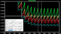
As explained in their research paper, the new technique leverages that quantum tunneling effects are independent of the frequency of the applied gate voltage square wave.
On the other hand, the desired charge pump current, as it relates to device defects, does correlate with gate voltage frequency.

NIST's Frequency modulated charge pumping. Image used courtesy of NIST
With that concept in mind, the researchers developed a new technique, dubbed “Frequency Modulated Charge Pumping,” in which two different square waves are applied to the FET’s gate, both at different frequencies.
Since the quantum contribution to charge pump current remains constant in both cases, the researchers can then subtract the two current signals from one another to arrive at their final result.
According to the researchers, the new technique successfully determined defects as small as the diameter of a hydrogen atom.
Taking Defect Detection to the Future
With this new technique for defect detection at advanced MOSFET nodes, the researchers have made a considerable contribution to the semiconductor industry.
By being able to accurately and easily detect transistor defects, engineers can detect and correct device defects, ensuring quality and higher performance semiconductors overall.
Though the shrinking of technology consistently brings up more and more challenges for electrical engineers, the future is hopeful with how many times researchers find ways of overcoming limitations.
Related Content