Facebook
 Google
 GitHub
 Linkedin
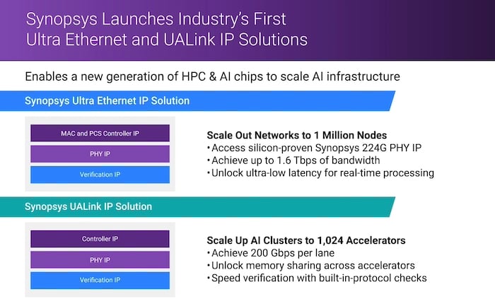
Synopsys Unveils ‘Industry’s First’ Ultra Ethernet and UALink IP
Unveiled today, Synopsys' two new IP solutions allow up to a million nodes, each with 1,024 accelerators.
Today, Synopsys announced the “industry’s first Ultra Ethernet IP and UALink IP solutions.” The two power-optimized interconnect solutions are designed to support very large AI accelerator clusters and are based on industry-standard architectures. They include controllers, physical layer (PHY), and verification IP.

Synopsys' two new solutions address the data-heavy demands of AI data centers. Image from Adobe Stock (under license)
Synopsys, long known as a provider of high-end silicon design tools, also has a large intellectual property (IP) library. The two new packages are the company's latest IP development in the high-speed data-center interconnect arena. The Ultra Ethernet node networking offers up to 1.6 Tbps with up to one million node endpoints. Within the nodes, the UALink delivers up to 200 Gbps per lane for up to 1,024 individual accelerators.
All About Circuits spoke to Ron Lowman, Synopsys' principal HPC IP product manager, to learn more about the implications of these two networking solutions.
Key Features of the New Networking IP
The Ultra Ethernet and UALink IP solutions are based on industry-accepted open standards. Synopsys says the f dual solution prioritizes energy efficiency, minimizes network congestion, and enables massing AI network scaling.

Synopsys offers its Ultra Ethernet and UALink products as a low-risk, standards-based approach to AI data center scaling. Image used courtesy of Synopsys
“What UALink and Ultra Ethernet do is really expand standard interfaces to scale up for local networks, specifically for homogeneous AI compute,” said Lowman.
UALink IP Solution
“UALink scales the networks up for a local network,” said Lowman. “This is an open industry standard to facilitate direct load store and atomic operations between accelerators. It's very focused on this particular function.”
Some of the key features of UALink include its:
- Support for up to 1,024 AI accelerators per node for high-density XPU-to-XPU networking
- Data transfer of 200 Gbps per lane
- Low latency with memory sharing
- Built-in protocol check for AI hardware verification
Ultra Ethernet IP Solution
“Ultra Ethernet is focused on scaling out Ethernet,” Lowman explained. “Again, it's an open standard to handle the high demands of massive AI networks.”
Some of the key features of Ultra Ethernet include its:
- Support for up to one million nodes
- Best-in-class 224-G Ethernet physical layer
- PHY, MAC, PCS controller, and verification IP
- Patented error correction (up to 1.6 Tbps)
- Easy integration with higher layers of Ethernet stack
Scaling Beyond Monolithic Processors
Synopsys' system of moving AI data between large numbers of accelerators and cluster nodes directly descends from a 1974 invention by Xerox PARC's Robert Metcalf. Metcalf wanted to connect a newly developed laser printer to multiple computers in the building. To do so, he needed a new protocol supporting multipoint connection with collision detection. The original system, dubbed Ethernet, was designed to connect a few hundred computers at most and reached speeds of 2.94 Mbps. Systems today must carry gigabits of data from tens or hundreds of thousands of data center clusters in a fast, efficient, and coordinated manner.
“We're in a phase where we actually are running these AI algorithms at scale. We're getting a lot of people actually operating and training more devices, so we worry about downtime of these data centers and the reliability of the hardware,” said Lowman. “It's just a nascent market. Both these standards are really essential to promote the growth of this space.”
The monolithic (all-in-one die) processing unit is no longer a viable component of high-performance computing (HPC) scaling. Solutions today include either chiplet-based processors or multiple accelerators of various types connected with high-speed networking. The accelerators may be graphics processing units (GPUs), tensor processing units (TPUs), neural processing units (NPUs), or other specialized processing units collectively referred to as XPUs.
Networking IP ready for maximum AI scaling. Image used courtesy of Synopsys
Even with chiplets and customized XPUs, silicon manufacturers are continuing to push limits in scale to achieve the best possible performance out of a given area of silicon. According to Lowman, the highest performers are reaching 5 or 4 nm and are pushing toward 3- and 2-nm process nodes. Even so, these node sizes will not be enough to keep up with AI scaling; devices must be networked on a massive scale to keep up with AI computing needs.
Low Risk for a Speed-Hungry Industry
AI model parameter numbers have been doubling every four to six months and are expected to continue for the foreseeable future. That’s about four times faster than Moore’s Law. While the power of the accelerators is continuing to increase, just improving the silicon isn’t enough. Much of computing power growth is being fulfilled by increasing the parallelism of cluster XPUs and cluster nodes. Doing so requires networking throughput commensurate with the number of accelerator end nodes. Synopsys' two new Ethernet IP sets allow the maximum possible AI data center scaling.
The new IP is available now for silicon producers to license in their AI data center solutions. Launch partners include AMD, Astera Labs, Juniper Networks, Tenstorrent, and XConn. As a complete solution supporting over a billion accelerators per networked system, the Synopsys IP is a low-risk way for hardware providers to develop and deliver massive AI server farms.