Facebook
 Google
 GitHub
 Linkedin
Widespread Micro-transfer Printing May Open the Floodgates for 3D ICs
Following a licensing agreement with X-Celeprint, X-FAB Silicon Foundries can now use a fabrication technique that will combine a wide range of semiconductors on a single 3D IC.
X-FAB Silicon Foundries recently announced that it will become the industry’s first foundry to use micro-transfer printing (MTP) at high volumes.
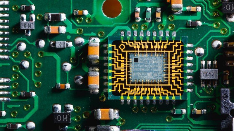
Micro-transfer printing (MTP) is a semiconductor fabrication process that involves integrating microscale electronic devices onto non-initial substrates. This fab process allows manufacturers to venture into a new territory of both two-dimensional and three-dimensional products.
Over the last several years, X-FAB, a company focused on analog/mixed-signal and specialty semiconductor solutions, has invested in MTP-based integration to optimize workflows and cleanroom protocols. Now, X-FAB will use MTP for mass production thanks to an agreement with X-Celeprint.
X-Celeprint licenses MTP technology and holds 300 patents to support semiconductor manufacturers adopting MTP. With MTP, X-FAB will be able to support heterogeneous integration of SOI, GaN, GaAs, InP, and MEMS.
How Does Micro-transfer Printing Work?
How does the MTP process work? Based on different process nodes, wafer sizes, and materials, MTP stacks and fans out thin dies. This technology then lifts and transfers 10-micron "x-chips" from a donor wafer to CMOS (or another surface). Many dies worth of these x-chips can adhere to an elastomeric transfer stamp in parallel.

This is an example of the transfer stamp of 16x16 dies, each containing 12x3 x-chips. This stamp is able to transfer 9,216 dies simultaneously from the source wafer to its destination. Image used courtesy of X-Celeprint
The spacing between the x-chips on the die allows for fanout, where the interleaved dies from the source wafer are transferred. One crucial aspect of MTP is the elastomer stamp made of polydimethylsiloxane (PDMS), which is a silicon-based organic polymer that creates a strong adhesive for the printing process. The stamp serves as a carrier, transferring arrays of devices from one substrate onto nearly any destination.
After the transfer is complete, the new substrate forms a virtually monolithic 3D stacked IC. 3D ICs are known to enhance performance, increase power efficiency, and yield a smaller footprint than conventional IC fabrication. MTP is also able to shorten time-to-market and save on manufacturing costs. This fabrication technology can be used for wafer-level integration of discrete components, passives, and different process technologies/nodes.

X-Celeprint offers a range of MTP printing tools and custom stamps for discrete and passive components on any substrate. Image used courtesy of X-Celeprint
Volker Herbig, the VP of X-FAB’s MEMS business unit, discussed how licensing for MTP technology through X-Celeprint will positively impact X-FAB’s future. “We can assist customers looking to implement complete multifunctional subsystems at the wafer level, even when there are high degrees of complexity involved," he explains. "Signal conditioning, power, RF, MEMS, and CMOS sensors, optoelectronic devices, optical filters, and countless other possibilities will all be covered.”
A Contrast to Epitaxial Growth and Wafer Bonding
There are other integration techniques commonly used in semiconductor fabrication, some of the most common being epitaxial growth and wafer bonding.
In the semiconductor world, epitaxial growth occurs when a thin film is grown epitaxially on a semiconductor substrate wafer. This technique is affordable since most fabs don’t have to outsource circuit fabrication. It also allows for uniformity in the substrate composition. Fab technicians can control growth parameters and gain a better understanding of the growth itself. However, epitaxial growth does have some limitations; desired substrates can only be in the micron dimensions.

Using chemical vapor deposition, epitaxial growth transfers a thin layer of single-crystal material over a single-crystal substrate. This process boosts the performance of bipolar devices. Image used courtesy of Wafer World
The other common fabrication process, wafer bonding, refers to a technique in which two mirror-polished wafers, indiscriminate of material, stick to one another through a number of bonding methods (adhesive bonding, anodic bonding, fusion bonding, glass frit bonding, etc). This process is conducted at room temperature. Used to fabricate MEMS, wafer bonding requires special protocols, including controlled energy flow and protection against environmental influences and heat dissipation.
The etching and deposition processes of epitaxial growth and wafer bonding are typically not up to the challenge of 2D or 3D-level IC design. These sought-after devices are flexible and stretchable, which is something only transfer printing can achieve.
Transfer Printing Techniques
Micro-transfer printing isn't the only kind of transfer printing technique. Some transfer printing techniques make use of a type of glue that modulates the interfacial adhesion strength for copying and printing.
Tape Transfer Printing
Tape transfer printing involves surface chemistry, using solvent releasable tapes as stamps. Because the adhesion between the tape and inks is extremely strong, manufacturers can reliably retrieve inks from the donor substrate. The problem with this is tape transfer can leave residue on inks that can ultimately degrade the device’s performance.

The working principle behind transfer printing. Image used courtesy of Nature
Kinetically Controlled Printing
Another technique is kinetically controlled printing. This process uses viscoelastic stamps to retrieve inks from the donor substrate at high velocity. It then transfers the ink to the receiving substrate at low velocity. Kinetically controlled printing has been used to fabricate flexible and stretchable inorganic electronics.
Despite these advantages, this technique is costly because it requires additional instruments for velocity control. Additionally, the adhesion is not as strong as other methods. Still, many fab houses consider kinetically controlled printing the most promising option because it is versatile and convenient.
Micro-transfer Printing
How does micro-transfer printing (MTP) compare to these other common transfer printing methods? MTP is a low-cost technique that can occur at room temperature and doesn't require solvents. This reduces the cleanroom protocols for temperature requirements and allows fab personnel to print on almost any type of substrate—glass, ceramics, plastics, and various semiconductors.

Applications of MTP. Image used courtesy of X-Celeprint
Additionally, a source wafer can go through the MTP process and still be reusable. For instance, the source wafer can be repurposed into solar cells, which decreases the environmental impact of fabrication.
X-FAB Uses MTP for BEOL Processing
X-FAB intends to use X-Celeprint’s MTP technology as its standard back-end-of-line (BEOL) processing, the second portion of IC fabrication where resistors, transistors, and capacitors are interconnected on a wafer using wires. The 3D ICs produced from MTP are said to find use in optoelectronics and silicon photonics, power management, RF communication, sensors, and hardware security applications.