Facebook
 Google
 GitHub
 Linkedin
MIT Pioneers Two-Chip Authentication to Secure Cryptographic Schemes
MIT's CMOS technique creates paired chips with identical “fingerprints” that secure hardware authentication without storing cryptographic keys on external servers.
MIT engineers recently unveiled a new concept for a chip-fabrication method that enables two integrated circuits to share a unique “fingerprint.” This new method would allow devices to authenticate each other directly, without the need for external servers.

MIT’s new technique allows two chips to share a unique fingerprint, enabling direct authentication without external servers.
Currently, most hardware authentication systems rely on physical unclonable functions (PUFs), unique electrical characteristics created by tiny variations during semiconductor fabrication. These variations act like a fingerprint for each chip and can be used to generate cryptographic keys.
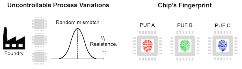
Physical unclonable functions (PUFs) rely on microscopic manufacturing variations that create a unique hardware fingerprint for each chip.
However, traditional PUF-based systems often require challenge-response data to be stored or enrolled on a third-party server. That architecture introduces potential attack points and increases communication overhead for low-power devices. The MIT researchers set out to remove that dependency by designing a system in which two chips share the same underlying randomness, enabling them to authenticate each other directly.
The Twin-Chip Authentication Concept
The research introduces what the team calls a “twin PUF” system, in which two chips are fabricated together so they share identical entropy. Rather than each device having a completely independent fingerprint, the two chips form a matched pair whose random structure is correlated.
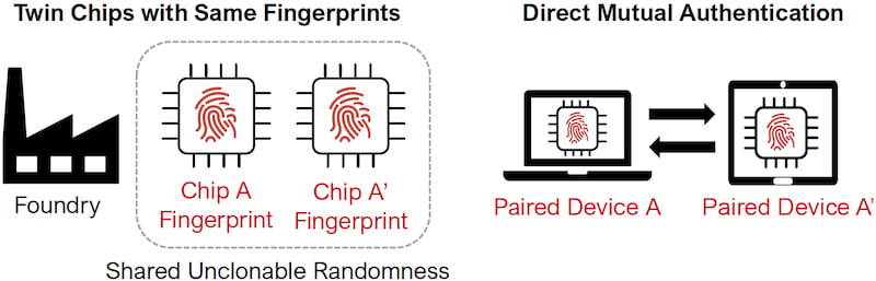
The twin-chip PUF architecture enables two paired devices to share the same physical randomness, allowing direct mutual authentication.
The idea is similar to tearing a piece of paper in half: each piece is unique, but the edges match perfectly. In the same way, two chips fabricated side-by-side can share randomness, allowing them to recognize one another.
Because the fingerprint is physically embedded in the silicon during manufacturing, the paired devices can authenticate each other directly without storing cryptographic secrets in memory or sending authentication requests to a remote server.
How the Twin PUF Hardware Works
The twin-chip authentication mechanism is implemented during the pre-wafer-dicing stage, when chips are still connected on the same silicon wafer.
In the prototype design, the researchers placed transistor structures along the edges of two adjacent dies and connected them using metal layers. When illuminated, on-chip photodiodes convert energy and drive circuits that intentionally induce gate-oxide breakdown in specific transistors. Because these transistors' breakdown times vary randomly due to manufacturing variations, the resulting electrical states form the PUF fingerprint.
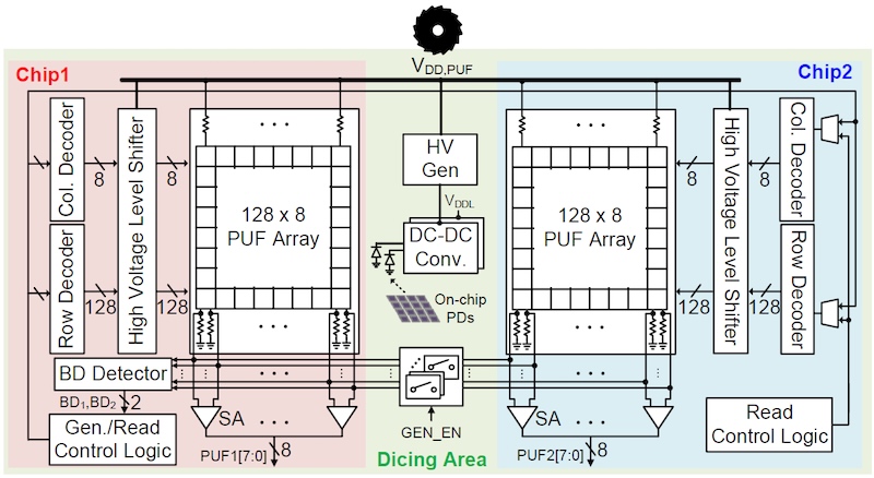
Block diagram of the twin PUF architecture showing paired PUF arrays, photovoltaic energy harvesting, and on-chip control circuitry.
In the twin configuration, four transistors across the two chips share the same breakdown event. When one transistor fails first, the circuit architecture ensures a complementary failure occurs on the paired chip. This creates matched but opposite responses that both devices can use for authentication.
The researchers fabricated prototype devices using a 65-nm CMOS process and implemented arrays of 128 × 8 PUF cells per chip. The generation process was powered entirely by photovoltaic energy harvested from LED illumination during wafer processing.
Measured results demonstrated:
- 98.4% average consistency between paired twin-chip fingerprints
- ~50% inter-die Hamming distance, indicating strong randomness
- 0.4% native bit-error rate
- Successful validation using the NIST SP 800-22 statistical randomness tests
These results indicate the twin PUF keys can be generated reliably and used for authentication without external key storage.
Potential Applications for Edge and Embedded Devices
The twin-chip authentication approach is particularly suited to systems where two devices must communicate securely but operate with limited computing resources.
Examples include:
- Medical sensor systems, such as ingestible diagnostic pills that are paired with wearable receivers
- Low-power IoT devices that cannot maintain persistent connections to authentication servers
- Secure edge computing nodes operating in constrained environments
- Paired industrial sensors or controllers that require hardware-level authentication
Since MIT’s new technique would rely upon conventional CMOS processes and simple LED illumination, it could be implemented within existing semiconductor manufacturing lines without major changes to fabrication workflows.
The new MIT prototype demonstrates that shared hardware fingerprints can be created using standard CMOS processes and basic optical illumination during wafer processing. If this new technique is scalable for large-scale production, it could enable safe device authentication without requiring external infrastructure. This hardware-level trust could benefit distributed edge systems that require secure communication with minimal computation and power.
All images used courtesy of MIT.
Related Content