Facebook
 Google
 GitHub
 Linkedin
Zero ASIC Develops First-Ever Open Standard eFPGA Product
Zero ASIC says its approach standardizes an eFPGA architecture in the same way that RISC-V did for CPUs and JEDEC did for memory.
Massachusetts-based fabless semiconductor startup Zero ASIC has launched Platypus, the so-called first open standard eFPGA IP for commercial use. The new product features a published architecture, open bitstream format, and toolchain support to reduce vendor lock-in and extend hardware lifespan in long-term embedded systems. Let’s take a look at how the company got here, what Platypus offers, and what might come next.
From Adapteva to Zero ASIC
Zero ASIC was founded by Andreas Olofsson in 2008 under the name Adapteva. Olofsson’s goal was aggressive: improve floating-point performance per watt by 10× for mobile devices. Within 14 months, he had a working prototype—a 65-nm chip with 16 independent RISC cores—and closed a $1.5 million Series A funding round from BittWare.
Adapteva’s core product offering was the Epiphany architecture, a scalable, manycore design with a flat 32-bit memory space shared by up to 4,096 cores. Unlike traditional CPUs, it avoided cache coherency entirely. Instead, each core had local memory, and the architecture used a mesh-style network-on-chip to pass data between cores.
From 2011 to 2016, Adapteva built out the Epiphany product line:
- Epiphany-III (2011): 16-core chip, 65 nm and 28 nm
- Epiphany-IV (2012): 64 cores, 28-nm GlobalFoundries process
- Epiphany-V (2016): 1,024-core, 64-bit version on a 16-nm node with 64 KB per core, double-precision support, and SIMD extensions for AI and cryptography
The company then launched Parallella, a Kickstarter campaign in 2012 that raised nearly $900,000. Backers got a $99 credit card–sized board with a 16-core Epiphany chip and a dual-core Arm processor (via Xilinx Zynq). Delivered in late 2013, it targeted education and open-source development. Though limited in scope, Parallella demonstrated that highly parallel systems could be democratized.
The Epiphany V chip, though technically impressive, never shipped widely. Olofsson took a DARPA role in 2017, and Adapteva’s commercial work paused. Over the next few years, the company rebranded to Zero ASIC, expanded its scope, and focused on chiplet platforms and tool automation.
Chiplets, Platforms, and Silicon Access
Zero ASIC’s shift from manycore computing to chiplet-based design came with a new thesis: custom silicon is too hard, too expensive, and too slow for most companies. To change that, the company launched the ChipMaker platform in 2023. ChipMaker offers pre-fabricated 3D chiplets with 128 Gb/s/mm² chiplet bandwidth, a 3D interposer delivering 512 Gb/s/mm bisection bandwidth for die-to-die links, and an open-source toolchain that supports Verilog, VHDL, Chisel, and Python for compiling eFPGA bitstreams.
Zero ASIC claims to be building "the world’s first composable chiplet platform." Image used courtesy of Zero ASIC
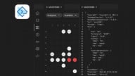
Logik, built on SiliconCompiler, integrates open tooling like Yosys, VPR, and Verilator. It automates RTL-to-bitstream compilation, reducing the time and tooling overhead typically associated with FPGA development. Ultimately, the company’s stated mission is to democratize access to silicon by enabling rapid assembly of system-in-package designs using off-the-shelf chiplets. The long-term bet is that building silicon should become as modular and flexible as writing software.
Platypus: Open eFPGA IP With a Standards-First Model
On March 18, 2025, Zero ASIC announced Platypus, described as the world’s first commercial eFPGA IP product built around open standards. What sets Platypus apart is its fully published FPGA architecture under the Apache License, an open-source bitstream format that removes vendor lock-in, and a toolchain—Logik—that supports a complete RTL-to-bitstream flow using open-source tools.
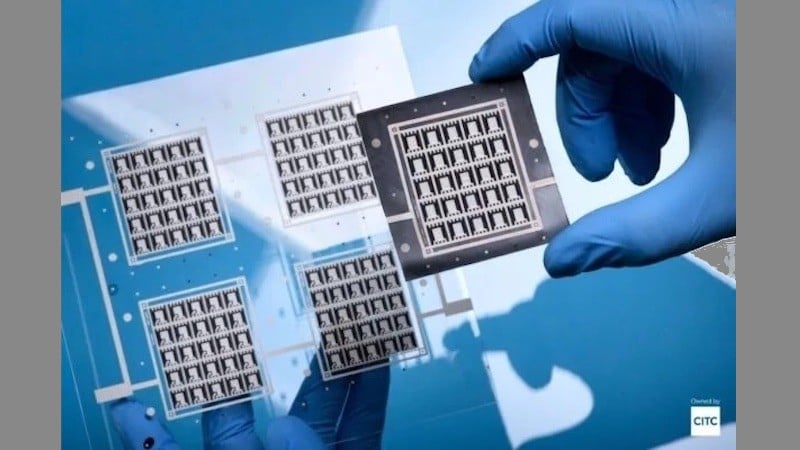
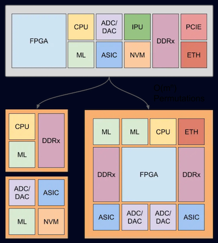
The first core in the family, the Z1000, is built on GlobalFoundries’ 12-nm LP process and includes 2,048 logic elements and 1,024 flip-flops. Larger cores, ranging from the Z1002 to Z1008, are on the roadmap and scale up to 131,072 logic elements.

The Z1000-GF12LP, a Z1000 standard eFPGA architecture, ported to GlobalFoundries' GF12LP process. Image used courtesy of Zero ASIC
Each Platypus hardened IP block is delivered with standardized memory-mapped interfaces—AXI, APB, or UMI—as well as soft RTL logic to manage reset, security, and bitstream loading. Integration materials include documentation, layout files, timing models, and simulation support, covering everything needed for design and tapeout.
Platypus is designed to solve the long-standing problem of FPGA obsolescence. In sectors like aerospace, defense, and industrial systems, hardware often needs to stay in use for decades. Over that time, FPGA vendors may phase out devices, change bitstream formats, or drop tool support entirely. When that happens, replacing a single component can mean redesigning entire subsystems.
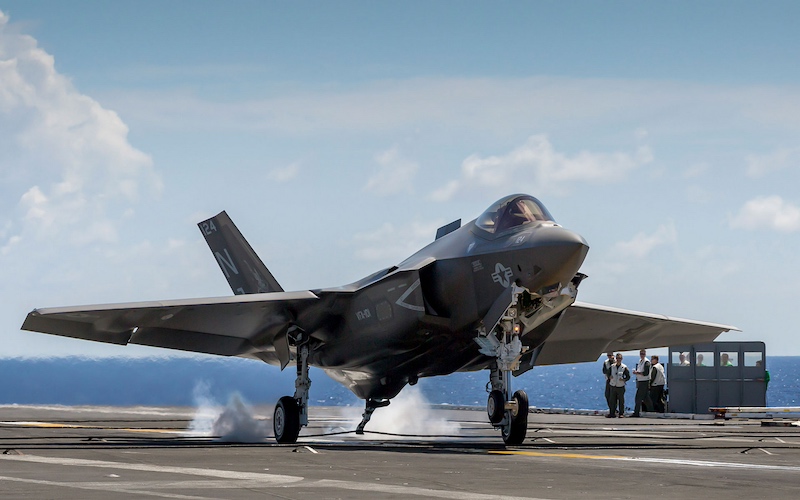
Zero ASIC uses the F-35 fighter jet program as an example of the mismatch between infrastructure timelines and fast-moving silicon roadmaps. Image used courtesy of Lockheed Martin
Zero ASIC points to the F-35 fighter jet program as a real-world example. While this program launched development in 1997, it didn’t enter full-rate production until 2021. During that span, six generations of FPGA architectures came and went, while transistor density increased by a factor of 10,000. That mismatch between long infrastructure timelines and fast-moving silicon roadmaps contributes to billions in non-recurring engineering costs, along with an increased risk of sourcing counterfeit parts.
Zero ASIC’s approach standardizes its eFPGA architecture in the same way that RISC-V did for CPUs and JEDEC did for memory. The goal is to let systems designers avoid vendor-specific constraints and extend the useful life of their products. The company sees Platypus as a foundational step toward making open, reusable FPGAs a long-term standard.
What’s Next?
Platypus IP cores are available now for early access. The company plans to release the FPGA Architect platform in Q2 2025, giving users the ability to define custom FPGA configurations per project.
Zero ASIC says it has secured funding through at least 2029 and is working with academic and government groups, including a University of Texas–led DoD research team on secure microelectronics and the Universal Chiplet Interconnect Express (UCIe) Consortium for open chiplet standards.
The roadmap extends from chiplets to toolchains to integration services. If the Platypus standard takes hold, it could define a new baseline for long-lived embedded designs where customization and longevity matter more than raw logic density.
Related Content