Facebook
 Google
 GitHub
 Linkedin
A Precision Multi-Sensor Data Acquisition Module
Build a low-noise, 32-bit delta-sigma ADC board designed around the ADS1262. This 10-channel design features integrated signal conditioning for RTDs, thermocouples, and strain gauges.
This 10-channel, 32-bit ADC converter is a low-noise, multiplexed delta-sigma (ΔΣ) analog-to-digital converter module built around the ADS1262 from Texas Instruments. It samples at 38 kSPS and integrates several features:
- A programmable gain amplifier (PGA).
- A 2.5 V low-drift voltage reference
- An internal oscillator
- Dual sensor-excitation current sources (IDAC)
- System-monitoring functions
- An auxiliary 24-bit ΔΣ ADC.
Together, these features enable precision measurement of strain gauges, weigh scales, pressure sensors, thermocouples, thermistors, and resistance temperature detectors (RTDs).
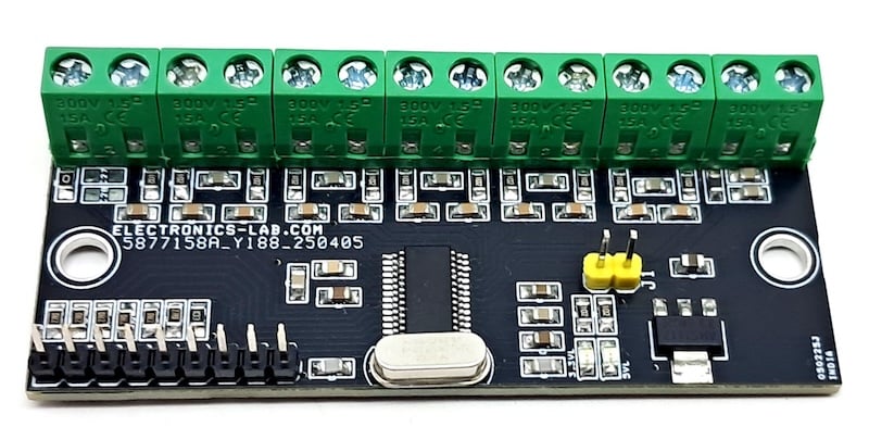
Figure 1. The assembled 10-Channel 32-Bit ADC Converter board, built around the ADS1262.
The ADS1262 provides 11 analog input pins: AIN0 through AIN9, plus a common input (AINCOM). These can be configured as up to five differential input pairs, ten single-ended inputs referenced to a common voltage, or a mix of both. A flexible input multiplexer routes any two inputs to the ADC's positive or negative input. Any AINx pin can also serve as a common input for single-ended measurements. AINCOM is purpose-built for this role, since it can supply a bias voltage to level-shift floating sensors into the PGA's common-mode range. All analog inputs are broken out to screw terminals on the board, with supporting filter and ratiometric circuitry for a variety of sensor types. Figure 1 shows the assembled board.
Specs and Features
- Power supply: 5 V DC (analog side), 3.3 V (digital side)
- Onboard 5 V and 3.3 V status LEDs
- Jumper to combine the 3.3 V LDO output with the 3.3 V digital supply
- Screw terminals for all analog inputs
- Header connector for the digital interface
- Precision 32-bit ΔΣ ADC plus an auxiliary 24-bit ΔΣ ADC (ADS1263)
- Data rates: 2.5 SPS to 38,400 SPS
- Differential input, CMOS PGA
- 11 multifunction analog inputs
- High-accuracy architecture: 1 nV/°C offset drift, 0.5 ppm/°C gain drift, 7 nVRMS noise (2.5 SPS, gain = 32), 3 ppm linearity
- 2.5 V internal voltage reference with 2 ppm/°C temperature drift
- 50 Hz and 60 Hz rejection
- Single-cycle settled conversions
- Dual sensor-excitation current sources and internal fault monitors
- 8 general-purpose inputs/outputs
- PCB dimensions: 72.39 mm x 33.66 mm
How It Works
The ADS1262 multiplexes its 11 analog inputs to the 32-bit primary ADC. The ADS1263 variant can also route them to an auxiliary 24-bit ADC. This lets a single device service up to five differential sensor channels or ten single-ended channels referenced to AINCOM.
Many of the input pins are multifunction. AIN0–AIN5 can serve as external reference inputs. All analog inputs can source the dual sensor-excitation currents (IDAC1 and IDAC2), each programmable from 50 µA to 3000 µA for biasing RTDs and thermistors. AINCOM provides the VBIAS level-shift function for single-supply operation. AIN3 through AINCOM also double as eight general-purpose I/O lines referenced to the 5 V analog supply.
An internal test DAC (TDAC) outputs known positive and negative voltages on AIN6 and AIN7 to diagnose the signal chain. These pins should not be loaded while the test signals are enabled, since the TDAC outputs are unbuffered.
A 7.3728 MHz crystal (X1) clocks the ADS1262's internal oscillator. An LM1117 3.3 V regulator (U2) derives the digital-side supply from the 5 V analog rail. Jumper J1 selects whether the two supplies are combined or separated.
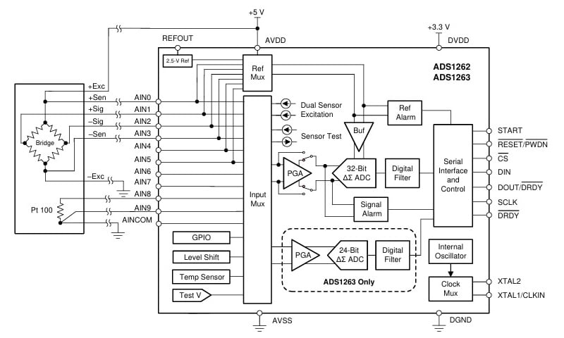
Figure 2. Temperature-compensated bridge measurement example using the ADS1262 showing the input multiplexer, PGA, dual ΔΣ ADCs, and support functions. Image used courtesy of Texas Instruments
Schematic and Bill of Materials
The full schematic for the 10-Channel 32-Bit ADC Converter is shown in Figure 3.
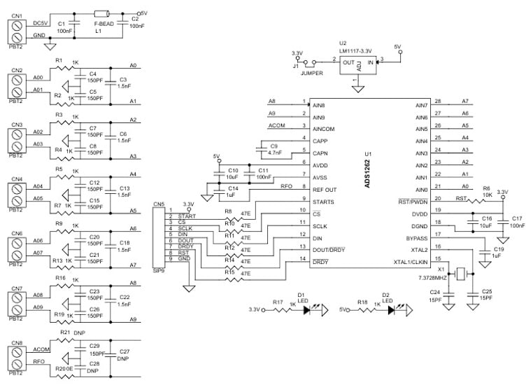
Figure 3. Schematic of the 10-Channel 32-Bit ADC Converter board.
The bill of materials is shown in Table 1.
Table 1. BOM for the 10-Channel 32-Bit ADC Converter.
| REF | DESCRIPTION | QTY | MFG | SUPPLIER | PART NO. |
| CN1, CN2, CN3, CN4, CN6, CN7, CN8 | 2 Pin Screw Terminal, Pitch 5.08 mm | 7 | Phoenix | Digikey | 277-1247-ND |
| CN5 | 9 Pin Male Header, Pitch 2.54 mm | 1 | Wurth | Digikey | 732-5322-ND |
| C1, C2, C11, C17 | 100 nF / 50 V Ceramic, SMD 0805 | 4 | Yageo/Murata | Digikey |
|
| C3, C6, C13, C18, C22 | 1.5 nF / 50 V Ceramic, SMD 0805 | 5 | Yageo/Murata | Digikey |
|
| C4, C5, C7, C8, C12, C15, C20, C21, C23, C26, C29 | 150 pF / 50 V Ceramic, SMD 0805 | 11 | Yageo/Murata | Digikey |
|
| C9 | 4.7 nF / 50 V Ceramic, SMD 0805 | 1 | Yageo/Murata | Digikey |
|
| C10, C16 | 10 uF / 25 V Ceramic, SMD 0805 | 2 | Yageo/Murata | Digikey |
|
| C14, C19 | 1 uF / 25 V Ceramic, SMD 0805 | 2 | Yageo/Murata | Digikey |
|
| C24, C25 | 15 pF / 50 V Ceramic, SMD 0805 | 2 | Yageo/Murata | Digikey |
|
| R21, C27, C28 | DNP | 3 |
|
|
|
| D1, D2 | LED, Red, SMD 0805 | 2 | Osram | Digikey | 475-1278-1-ND |
| J1 | 2 Pin Male Header, Pitch 2.54 mm | 1 | Wurth | Digikey | 732-5315-ND |
| L1 | Ferrite Bead, 150 Ohm / 1 A, SMD 0805 | 1 | Laird | Digikey | 240-2384-1-ND |
| R1-R5, R7, R9, R13, R16-R19 | 1 K | 12 | Yageo/Murata | Digikey |
|
| R6 | 10 K | 1 | Yageo/Murata | Digikey |
|
| R8, R10, R11, R12, R14, R15 | 47 Ohm | 6 | Yageo/Murata | Digikey |
|
| R20 | 0 Ohm | 1 | Yageo/Murata | Digikey |
|
| U1 | ADS1262, TSSOP-28 | 1 | TI | Digikey | 296-48477-1-ND |
| U2 | LM1117-3.3V | 1 | TI | Digikey | LM1117MP-3.3/NOPBCT-ND |
| X1 | 7.3728 MHz Crystal | 1 | CTS | Digikey | CTX1035-ND |
| J1-Shunt | Shunt | 1 | Sullins Connect | Digikey | S9001-ND |
Connections
Figure 4 shows how power, analog inputs, and the digital interface connect to the board.
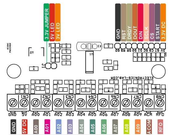
Figure 4. Connection diagram for the 10-Channel 32-Bit ADC Converter board.
CN1 — Power Input (2-pin, 5.08 mm pitch):
- Pin 1 = 5 V DC Input
- Pin 2 = GND
CN2 — Analog Inputs 0/1 (2-pin, 5.08 mm pitch):
- Pin 1 = Analog 00 Input
- Pin 2 = Analog 01 Input
CN3 — Analog Inputs 2/3 (2-pin, 5.08 mm pitch):
- Pin 1 = Analog 02 Input
- Pin 2 = Analog 03 Input
CN4 — Analog Inputs 4/5 (2-pin, 5.08 mm pitch):
- Pin 1 = Analog 04 Input
- Pin 2 = Analog 05 Input
CN6 — Analog Inputs 6/7 (2-pin, 5.08 mm pitch):
- Pin 1 = Analog 06 Input
- Pin 2 = Analog 07 Input
CN7 — Analog Inputs 8/9 (2-pin, 5.08 mm pitch):
- Pin 1 = Analog 08 Input
- Pin 2 = Analog 09 Input
CN8 — Common / Reference (2-pin, 5.08 mm pitch):
- Pin 1 = ACOM / Analog Common
- Pin 2 = Reference Output
CN5 — Digital Interface (9-pin header, 2.54 mm pitch):
- Pin 1 = 3.3 V DC Input
- Pin 2 = Start
- Pin 3 = CS
- Pin 4 = SCLK
- Pin 5 = DIN
- Pin 6 = DOUT
- Pin 7 = DRDY
- Pin 8 = RST
- Pin 9 = GND
D1 / D2 — Power LEDs:
- D1: 3.3 V power indicator
- D2: 5 V power indicator
J1 — 3.3 V Supply Select Jumper:
- Selects between internal LDO-derived 3.3 V or an external 3.3 V supply
PCB Files
The PCB measures 72.39 mm x 33.66 mm. The silk screen, top layer, and bottom layer are shown in Figure 5.
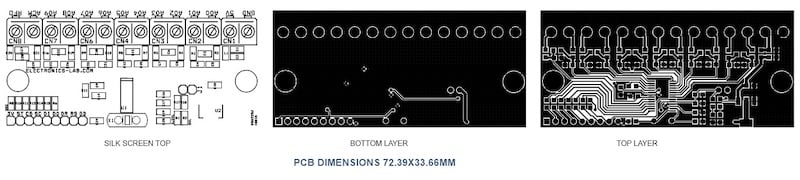
Figure 5. PCB layout for the 10-Channel 32-Bit ADC Converter, showing silk screen, top layer, and bottom layer.
You can download the layout files for this project here:
Data Acquisition Module Gerber Files
Except where noted, all images used courtesy of Rajkumar Sharma