 Facebook
 Google
 GitHub
 Linkedin
Make a PWM Driver for FPGA and SoC Design Using Verilog HDL
An FPGA is a crucial tool for many DSP and embedded systems engineers. However, the learning curve when getting started can be fairly steep. This project introduces the Quartus II and ModelSim software suites as well as a background on FPGA design flow for system on chip development. The development board used was a Terasic DE1-SoC, which has the Altera Cyclone V SoC chip. This IC contains an FPGA and an integrated ARM Cortex A9 as a hard processor system.
An FPGA is a crucial tool for many DSP and embedded systems engineers. However, the learning curve when getting started can be fairly steep. This project introduces the Quartus II and ModelSim software suites, as well as a background on FPGA design flow for System on Chip development. The development board used is a Terasic DE1-SoC, which has the Altera Cyclone V SoC chip. This IC contains an FPGA and an integrated ARM Cortex A9 as a hard processor system.
The FPGA Design Flow

The DE1-SoC System Builder

The System Builder software isn’t strictly necessary, but it is incredibly useful. The user names the project and selects which inputs / outputs will be used on the FPGA. This software will generate four different files in the selected directory. In this case, the project was titled"‘DE1_SOC_PWM" and only the external clock, LEDs and switches are used. The following files were generated:
- DE1_SOC_PWM.qpf Quartus Project File
- DE1_SOC_PWM.qsf Quartus Settings File
- DE1_SOC_PWM.v Verilog Top File
- DE1_SOC_PWM.sdc Synopsis Design Constraints
The quartus project file contains basic information about the project (e.g. the version of quartus that was used to create the project). The Quartus settings file contains information about all assignments made in the project. The top file is the top level entity in the hierarchical design, more will be said about this later. The synopsys design constraints file contains various constraints (such as timing).
Getting Started with the Project
This project was completed in Quartus Prime, but any version from 13.1 onwards will work, through the steps may change very slightly. Open the project by double clicking the .qpf file in your chosen directory
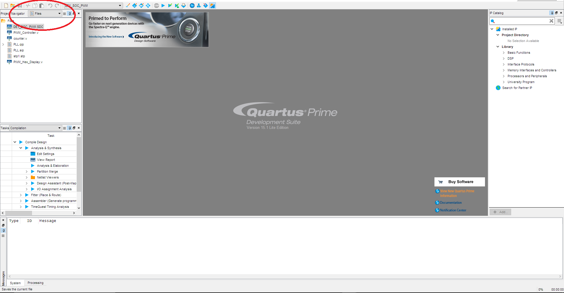
In the project navigator, select files and open the file called ‘[your_Project_Name].v’, it should open something similar to the following:
//=======================================================
//  This code is generated by Terasic System Builder
//=======================================================

module DE1_SOC_PWM(

	//////////// CLOCK //////////
	input 		          		CLOCK_50,
	input 		          		CLOCK2_50,
	input 		          		CLOCK3_50,
	input 		          		CLOCK4_50,

	//////////// SEG7 //////////
	output		     [6:0]		HEX0,
	output		     [6:0]		HEX1,
	output		     [6:0]		HEX2,
	output		     [6:0]		HEX3,
	output		     [6:0]		HEX4,
	output		     [6:0]		HEX5,

	//////////// LED //////////
	output		     [9:0]		LEDR,

	//////////// SW //////////
	input 		     [9:0]		SW
);


//=======================================================
//  REG/WIRE declarations
//=======================================================

//=======================================================
//  Structural coding
//=======================================================

endmodule
We will use this as the top file in our hierarchical design. What is meant by hierarchical design will become obvious as we add some more modules later on. If we look at the pin planner:
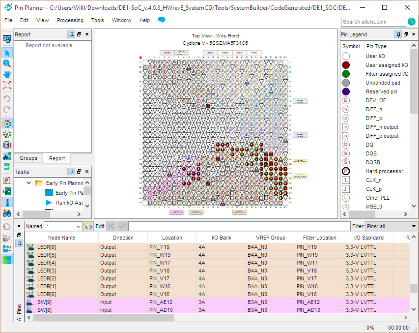
We can see that the pin assignments for the inputs and outputs in the top file have been done for us. This is one of the benefits of the using the system builder software, as this step can be quite lengthy and tedious.
Adding a PLL
The first step in designing our PWM driver is to implement a phase locked loop to generate a 5 MHz clock from the external 50 MHz oscillator. The Cyclone V SoC has dedicated hardware PLLs. To use one of these, an Altera IP PLL module can be used. The IP catalog (called MegaWizard Plugin Manager in in version 13.1) can be found in the tools menu. In the IP catalog, go to Basic Functions > Clocks and PLLs > Altera PLL. The following window should open after you name the PLL (in this case, named PLL)

For the Cyclone V SoC the speed grade is 6. If a different FPGA / SoC is used, the speed grade can be found in the datasheet. The reference clock on the DE1-SoC board is 50 MHz, and the desired output for the PWM driver is 5 MHz.
After the PLL IP has been generated, we’re going to include this as a module in the top file. To add a module in the top file, the following code template can be used:
Module_Name Module_Name_instance(
		.var1NameInModule 	(var1NameInCurrentFile),
		.var2NameInModule 	(var2NameInCurrentFile),
		...
                ...
                ...
	);
In the case of the PLL, there are three inputs and outputs. In the project navigator, under files open the PLL.v (under PLL.qip) to see the names of the nodes in the PLL module as the names may differ depending on the version of Quartus.
PLL PLL_inst(
		.refclk (CLOCK_50),    //  Input Clock
		.rst (1'b0),           //   Reset
		.outclk_0 (clk)        // 5 MHz Output Clock
	);
The input to the PLL is the external 50 MHz oscillator (connected to the port named CLOCK_50), which is used as the reference clock. As the reset is not used in this design, this is tied to a logic level 0 (i.e. does not reset). The output from this module (the 5 MHz clock) has been tied to a wire named clk. To add in this the module, the wire keyword is used.
$$ wire clk; $$
A wire is a type of structural net in Verilog, and is mostly used for combinational logic. In this case, it is going to be used for connecting the PLL to other module in the top file.
The PWM Driver
Now the PLL IP has been generated, we can move on to the next step, which is to design and verify our PWM driver module. The PWM driver will contain three major parts, a sawtooth generator, a comparator and a PWM code word.


While the output of the sawtooth generator is less than the PWM codeword, the output of the PWM pin is 1 and zero otherwise. Implementing the sawtooth generator in digital hardware is fairly straightforward as it's a simple counter. For an n-bit PWM driver, an n-bit counter is required. The counter will take 2n clock cycles to reset, and thus each PWM cycle is 2n clock cycles long. The duty cycle can be calculated as the number of clock cycles the PWM output is high, over the number of clock cycles one PWM cycle requires.
Verilog Implementation of PWM Driver
As mentioned before, there are three major parts to the PWM driver: an n-bit counter, a PWM codeword, and a comparator. We’ll start with the 8 bit counter.
`timescale 1ps / 1ps
module counter (
	clk,				//Counter clock
	counter_out   			 // 8 bit output from the counter
);

	input clk;			// clock declared as an input port
	output reg [7:0] counter_out;  // counter_out declared as an 8 bit output register

	always @(posedge clk)
		begin
			counter_out <= #1 counter_out + 1'b1;
		end

endmodule				// identifies the end of the module
Modules are the basic building blocks of a hierarchical design in Verilog. First, ports are declared, and are then specified if it is an input, output or inout port. The next bit of code is an always block. The sensitivity list, (posedge clk in this case) is the trigger of when the code inside the begin/end block is executed. The begin and end block is similar to the { } in the C programming language.

Now the counter is finished, we can write the PWM driver module. The following code is used:
`timescale 1ps / 1ps
module PWM_Controller (
	PWM_CW,               // Ports declared
	PWM_out,
	clk
	);

	input clk;            //Port type declared
	input [7:0] PWM_CW;   // 8 bit PWM input

	output reg PWM_out; // 1 bit PWM output
	wire [7:0] counter_out;  // 8 bit counter output


	always @ (posedge clk)
	begin

			if (PWM_CW > counter_out)
				PWM_out <= 1;

			else
				PWM_out <= 0;
	end


	counter counter_inst(

		.clk (clk),
		.counter_out (counter_out)
		);

endmodule
This module is quite intuitive, as it simply compares the 8 bit counter output with the 8 bit PWM codeword, and sets the PWM output high or low depending on the value of the counter. Notice how the non-blocking assignments (<=) are used rather than blocking (=). As a general rule, when writing sequential logic, the non-blocking assignment should be used, and for combinational the blocking should be used.
Verifying the PWM driver
There are two main types of simulations used in FPGA development. RTL (register transfer level) simulations are used to verify the design before logic synthesis, i.e. how the Verilog code behaves. Gate-Level simulations are used post synthesis, and post fitting stages, i.e. simulates how signals will act on the FPGA or ASIC. The latter requires a lot more time to simulate.
RTL Simulation
The ModelSim Altera Edition software will be used to perform the RTL simulation of the PLL. Before this can be done, a testbench is required. A testbench is similar to the top file, but is used for verification.
Create a new project in ModelSim, and make it the same directory as the Quartus project file. Add the existing PWM driver and counter modules and compile them. Add a new verilog file to the same directory and call it [module_under_test]_tb.v.
`timescale 1ps / 1ps
module PWM_tb;


reg clk;
wire PWM_out;
wire [7:0] counter_out;
reg [7:0] PWM_CW;

assign counter_out = PWM_inst_1.counter_inst.counter_out;

parameter CYCLE = 200000;
parameter HALF_CYCLE = 100000;

initial
begin
  clk=1'b0;
  PWM_inst_1.counter_inst.counter_out=8'b0;
  PWM_CW=8'b00110000;
end

always
	begin
		#CYCLE clk = !clk;
	end


PWM_Controller PWM_inst_1 (
	.clk (clk),
	.PWM_CW (PWM_CW),
	.PWM_out (PWM_out)
);

endmodule
The timebase for the simulation is 1 ps, so #1 is a 1 ps delay. To generate a 5 MHz clock, it’s cycle should be described in ps, which is 200 ps. From this, we can generate a test clock, which can be seen in the always block. When a digital circuit is synthesized, it will have an initial value at t=0. This is not the case for an RTL simulation, so all registers must be wrote with an initial value. This is done in the initial block. Also note there are no ports in a testbench.
Running the Simulation
Once all the files have been compiled in modelsim, the design can be simulated. Select the testbench file from the start simulation window.

Although we haven’t used any Altera IP blocks in the PWM module, It’s worth mentioning how to simulate with Altera IP. In the libraries tab, select the relevant libaries to the IP, and include the .vo file to your project files. The .vo file is a functional description (RTL) of the IP.

Once the relevant libraries and testbench file is added, press ok to start the simulation. In the simulation tab, right click the PWM instance, and add to wave.

Run the simulation for around 20 us, and the simulation should look like the above figure.
Programming the FPGA
As our design has been verified, we can program the FPGA. Before we can do this, we need to update our top file.
//=======================================================
//  This code is generated by Terasic System Builder
//=======================================================

module DE1_SOC_PWM(

	//////////// CLOCK //////////
	input 		          		CLOCK_50,
	input 		          		CLOCK2_50,
	input 		          		CLOCK3_50,
	input 		          		CLOCK4_50,

	//////////// SEG7 //////////
	output		     [6:0]		HEX0,
	output		     [6:0]		HEX1,
	output		     [6:0]		HEX2,
	output		     [6:0]		HEX3,
	output		     [6:0]		HEX4,
	output		     [6:0]		HEX5,

	//////////// LED //////////
	output		     [9:0]		LEDR,

	//////////// SW //////////
	input 		     [9:0]		SW
);


//=======================================================
//  REG/WIRE declarations
//=======================================================

wire PWM_out;
wire clk;

assign LEDR[0] = PWM_out;
assign HEX0 = 7'b1111111;		 // Active low
assign HEX1 = 7'b1111111;
assign HEX2 = 7'b1111111;
assign HEX3 = 7'b1111111;
assign HEX4 = 7'b1111111;
assign HEX5 = 7'b1111111;

//=======================================================
//  Structural coding
//=======================================================

PWM_Controller PWM_inst_1 (
	.clk (clk),
	.PWM_CW (SW [7:0]),
	.PWM_out (PWM_out)
);

PLL PLL_inst(
		.refclk (CLOCK_50),  //  Input Clock
		.rst (1'b0),         //   Reset
		.outclk_0 (clk)      // 5 MHz Output Clock
	);


endmodule
Here, the top file is connecting the PLL output clock to the input clock to the PWM controller module, as well as connecting the output from the PWM controller to LED0 on the DE1 board. The PWM codeword is set by using switches 0 - 7.
Before flashing the device, it’s also worth looking the RTL viewer as an additional check for your design. This option is under Tools > Netlist Viewers > RTL Viewer

After confirming this, flash the device by using the programmer tool in Quartus (make sure the USB blaster driver is installed!)

Shortly after pressing start, the FPGA will be flashed. The brightness of the LED will change depending on the switches 0 to 7 on the DE1-SoC board.
Give this project a try for yourself! Get the BOM.


Your project is very nice…
I want to adjust the FPGA PWM with an external potentiometer, can you help me?
Thanks! This is very helpful =)