Facebook
 Google
 GitHub
 Linkedin
An Ultra-Low-Noise Pre-Amp For Audio Applications
Build an ultra-low-noise preamplifier with a JFE150 JFET and OPA202 op-amp, perfect for high-impedance sensors, hydrophones, guitar pickups, microphones, and turntables.
This compact preamplifier module is designed to amplify small signals from high-source-impedance sensors with minimal added noise. It delivers a midband gain of 60 dB and a flat frequency response from approximately 16 Hz to 43 kHz. The clean roll-off at the corner frequencies produces a natural-sounding filter response well suited to audio applications.
Figure 1 shows the fully assembled board. The circuit combines a discrete JFE150 N-channel junction field-effect transistor (JFET) first stage with a Texas Instruments OPA202 precision op-amp second stage.
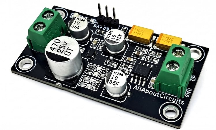
Figure 1. Assembled ultra-low-noise pre-amp PCB.
The board operates from a single 12 V DC supply by default, with an option for dual-supply operation via component substitution. Screw terminals are provided for signal input (CN2) and output (CN3). A 3-pin header (CN1) accepts the power supply connections.
Specs and Features
- Power supply: 12 VDC (single supply, default)
- Dual-supply operation supported via optional component population
- Voltage gain: 1000 V/V (60 dB)
- Frequency response: ~16 Hz to 43 kHz (−3 dB)
- Input stage IC: JFE150 JFET, SOT23-5 package
- Output stage IC: OPA202 precision op-amp, SOIC8 package
- Screw terminals (5.08 mm pitch) for signal input and output
- 3-pin male header (2.54 mm pitch) for power input
- On-board power LED (D1)
- Mounting holes: 4 × M3
- PCB dimensions: 54.93 × 29.05 mm
How It Works
Figure 2 shows the schematic for the ultra-low-noise pre-amp module.
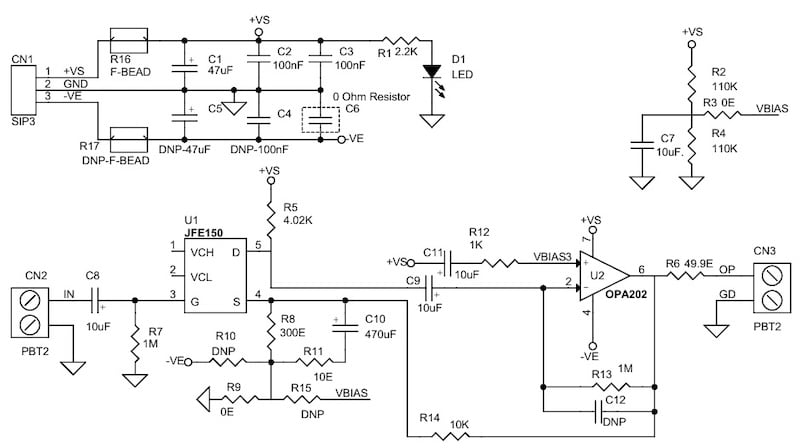
Figure 2. Schematic for the ultra-low-noise pre-amp.
The input signal is AC-coupled through C8 (10 µF) to the gate of U1 (JFE150). Resistor R7 (1 MΩ) sets the DC gate bias.
The JFE150's drain current is proportional to the gate voltage: IDS = gm × VGS. Therefore, it is an effective current-controlled transconductance element. The DC drain bias is set by R5 (4.02 kΩ), which is connected to the +VS rail.
The OPA202 (U2) is configured as a transimpedance amplifier. Its inverting input is driven by the JFET drain current, and feedback resistor R13 (1 MΩ) sets the transimpedance gain.
The non-inverting input is biased by a resistor divider (R2 and R4, both 110 kΩ) that sits at mid-supply (~6 V) in single-supply mode. This VBIAS shifts the OPA202 output DC level to approximately 6 V, keeping it within its linear range on a single rail.
Output isolation resistor R6 (49.9 Ω) improves stability when driving capacitive loads above 1 nF. It can be removed if no capacitive load drive is required.
Power-supply filtering is handled by a ferrite bead (R16, 600 Ω at 100 MHz) in series with the supply rail, supplemented by bulk (C1, 47 µF tantalum) and bypass capacitors (C2, C3, 100 nF each).
Bill of Materials
The bill of materials is shown in Table 1.
Table 1. BOM for the ultra-low-noise pre-amp.
| REF | DESCRIPTION | QTY | MFG | SUPPLIER | PART NO. |
| CN1 | 3 Pin Male Header, 2.54mm Pitch | 1 | WURTH | DIGIKEY | 732-5316-ND |
| CN2, CN3 | 2 Pin Screw Terminal, 5.08mm Pitch | 2 | PHOENIX | DIGIKEY | 277-1247-ND |
| C1 | 47uF/16V Tantalum, 7x4.3mm | 1 | KEMET | DIGIKEY | 399-3794-1-ND |
| C2, C3 | 100nF/50V Ceramic SMD 0805 | 2 | YAGEO/MURATA | DIGIKEY | |
| C4 | DNP — 100nF for Dual Supply, Ceramic SMD 0805 | 1 | YAGEO/MURATA | DIGIKEY | |
| C5 | DNP — 47uF for Dual Supply, Tantalum (same as C1) | 1 | DIGIKEY | ||
| C6 | 0 Ohm Resistor (default); 100nF for Dual Supply, Ceramic SMD 0805 | 1 | YAGEO/MURATA | DIGIKEY | |
| C7 | 10uF/25V Ceramic SMD 0805 | 1 | YAGEO/MURATA | DIGIKEY | |
| C8, C9, C11 | 10uF/25V Electrolytic SMD | 3 | NICHICON | DIGIKEY | 493-2185-1-ND |
| C10 | 470uF/25V SMD Electrolytic | 1 | NICHICON | DIGIKEY | 399-3794-1-ND |
| C12 | DNP | 0 | |||
| D1 | LED Red SMD 0805 | 1 | OSRAM | DIGIKEY | 475-1278-1-ND |
| R1 | 2.2K 5% SMD 0805 | 1 | YAGEO/MURATA | DIGIKEY | |
| R2, R4 | 110K 1% SMD 0805 | 2 | YAGEO/MURATA | DIGIKEY | |
| R3, R9 | 0Ω 5% SMD 0805 | 2 | YAGEO/MURATA | DIGIKEY | |
| R5 | 4.02K 1% SMD 0805 | 1 | YAGEO/MURATA | DIGIKEY | |
| R6 | 49.9Ω 1% SMD 0805 | 1 | YAGEO/MURATA | DIGIKEY | |
| R7, R13 | 1M 5% SMD 0805 | 2 | YAGEO/MURATA | DIGIKEY | |
| R8 | 300Ω 5% SMD 0805 | 1 | YAGEO/MURATA | DIGIKEY | |
| R10, R15 | DNP | 2 | |||
| R11 | 10Ω 5% SMD 0805 | 1 | YAGEO/MURATA | DIGIKEY | |
| R12 | 1K 5% SMD 0805 | 1 | YAGEO/MURATA | DIGIKEY | |
| R14 | 10K 5% SMD 0805 | 1 | YAGEO/MURATA | DIGIKEY | |
| R16 | Ferrite Bead 600Ω SMD 0805 | 1 | LAIRD | DIGIKEY | 240-2390-1-ND |
| R17 | DNP — Ferrite Bead for Dual Supply | 1 | LAIRD | DIGIKEY | |
| U1 | JFE150, SOT23-5 | 1 | TI | DIGIKEY | 296-JFE150DBVR-ND |
| U2 | OPA202, SOIC8 | 1 | TI | DIGIKEY | 296-51494-1-ND |
Connections
The connection diagram in Figure 3 shows all input and output assignments.
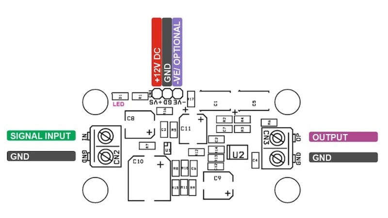
Figure 3. Connection diagram for the ultra-low-noise pre-amp.
CN1 — Power Header (3-pin, 2.54 mm pitch):
- Pin 1 = +VS (12 VDC)
- Pin 2 = GND
- Pin 3 = −VE (optional, dual-supply operation only)
CN2 — Signal Input (2-pin screw terminal, 5.08 mm pitch):
- Pin 1 = Signal Input (VIN)
- Pin 2 = GND
CN3 — Signal Output (2-pin screw terminal, 5.08 mm pitch):
- Pin 1 = Signal Output (VOUT)
- Pin 2 = GND
D1 — Power LED:
- Illuminates when +VS is applied
PCB Files
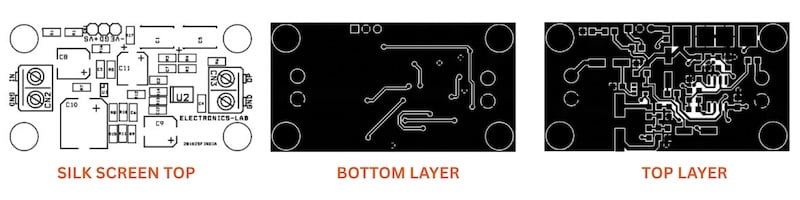
Figure 4. PCB layout: top silk screen, bottom copper layer, top copper layer.
Ultra-Low-Noise Pre-Amp Module Gerber Files
You can download the layout files for this project here:
Ultra-Low-Noise Pre-Amp Gerber Files
All images used courtesy of Rajkumar Sharma.