 Facebook
 Google
 GitHub
 Linkedin
High-Speed Waveform Generation with an MCU and a DAC
In this article, we’ll evaluate different firmware strategies in our pursuit of maximum-frequency analog signal generation.
In this article, we’ll evaluate different firmware strategies in our pursuit of maximum-frequency analog signal generation.
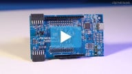
This is the second project article based on a custom-designed arbitrary waveform generator (AWG) built around a C8051F360 MCU and a TxDAC from Analog Devices.
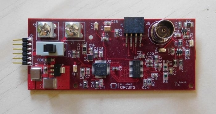
The previous article presents a firmware framework for convenient, high-speed transfer of parallel data from a microcontroller to a DAC. In that article you will also find links to four technical articles that explore the AWG’s schematic design and PCB layout.
Objective
Our goal in this project is to determine the maximum rate at which we can update the DAC output. This information then leads us to considerations regarding the highest obtainable waveform frequency. The maximum frequency of the system is by no means amazing when compared to the capabilities of high-performance digital synthesis systems, but in my opinion it is quite impressive in the context of a low-cost, moderately complex circuit that is flexible, extensible, and easy to use.
We have a lot to cover, so let’s jump right in.
Reading from Code Memory
The first strategy that we’ll assess is using the MCU’s flash memory to store the DAC data. Why use flash when we have RAM? Well, because MCUs usually (or nowadays maybe always) have more flash than RAM. Sometimes much more—for example, the C8051F360 has 32 kB of flash and only 1024 bytes of XRAM.
But what is the advantage of storing so much DAC data? Why can’t we just store enough data points for one cycle and then repeat? Well, that is an option, but having a (much) longer data buffer can be very advantageous in certain situations. For example, if you’re transferring packetized data, you might be able to store an entire packet’s worth of DAC data, which means that the MCU doesn’t have to generate waveform values. Rather, it just reads the values from memory, and this of course conserves processor resources. This concept can be extended to the generation of complex waveforms such as a chirp signal—better to calculate the chirp data elsewhere and store it in the MCU’s memory, rather than forcing the MCU to calculate the chirp-waveform values.
I implemented the code-memory-based technique by using Excel to generate waveform values and then storing them in a code-space array:
unsigned char code DACdata_128SPP[DACDATA_LEN] = {
		128,
		134,
		140,
		146,
		152,
		158,
		165,
		170,
                ...,
                ...,
                ...
};
I used an 8192-byte array, and the externally generated data corresponds to 64 cycles of a sine wave with 128 samples per period. As explained in the previous article, the critical parameter is the amount of time required to complete all of the instructions in the DAC-update interrupt service routine (ISR):
SI_INTERRUPT(INT0_ISR, INT0_IRQn)
{
	DEBUG_PORT |= REDLED;

	DAC_WORD = DACdata_128SPP[DACdata_index];

	DACdata_index++;
	if(DACdata_index == DACDATA_LEN)
	{
		DACdata_index = 0;
	}

	DEBUG_PORT &= ~REDLED;
}
Thus, we will evaluate our firmware techniques by activating a debug signal at the beginning of the ISR and deactivating it at the end of the ISR. We then probe the signal, and the width of the positive pulse gives us some information about the ISR execution time and, by extension, the maximum DAC update rate. Note that I’m running the MCU at its maximum processor frequency, i.e., 100 MHz. Here is a representative scope capture:
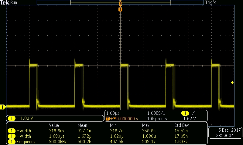
So the read-from-code approach gives us an average ISR execution time of about 325 ns (it’s actually not quite that simple, as we’ll see later). Notice the jitter on the falling edge. The scope is triggering on the rising edge, and the variation in the location of the falling edge shows us that the ISR execution time is not perfectly constant.
Here’s another scope capture; you might find this one interesting, as it shows the relationship between ISR execution and the change in the DAC voltage. You can also see how the “staircase” pattern is more evident in the higher-slope portions of the sinusoid.
Reading from XRAM
Storing DAC data in code space gives us the advantage of longer buffers, but is this approach slowing us down? The issue here is whether reading data from flash takes significantly longer than reading data from XRAM.
This new firmware configuration uses a 384-byte XRAM array to store 3 cycles of a sine wave with 128 samples per period. I generate the values externally and store them in a 384-byte code-space array, then I copy all the values into the XRAM array. I had to do it this way because the compiler wouldn’t allow me to initialize the XRAM array in the same way that I initialize the code-space array (actually it did allow me to, but then the program would just crash upon execution). Here is the code:
unsigned char xdata DACdata_RAM[DACDATA_LEN];

unsigned char code DACdata_128SPP[DACDATA_LEN] = {
		128,
		134,
                ...,
                ...
};
for(n=0; n
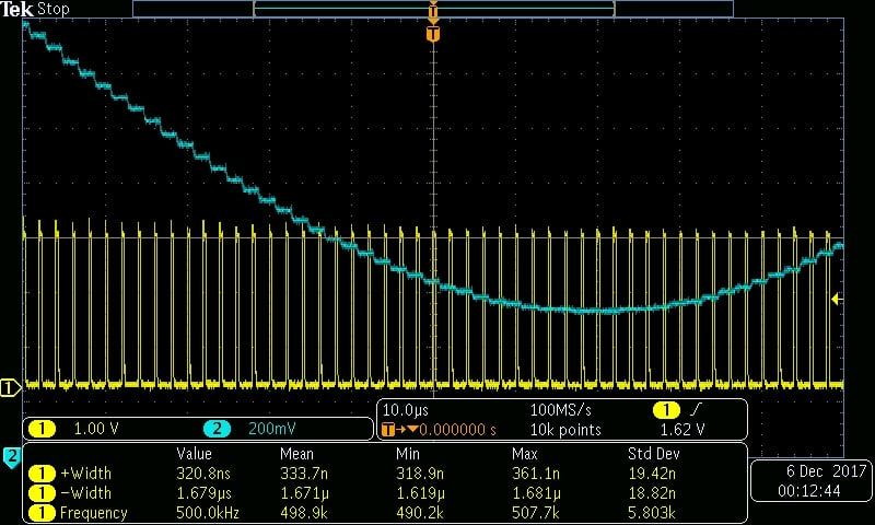
As you can see in the following scope capture, this technique has indeed decreased the ISR execution time.
<img alt="" src="https://www.allaboutcircuits.com/uploads/articles/proj_AWG2_scope3.jpg" />
This reduction is significant, but not amazing. I did a careful comparison between the two techniques, and the average positive pulse widths were 329 ns when reading from code and 310 ns when reading from XRAM.
So where do we stand? Let’s take the reading-from-XRAM measurement and add a bit of margin—say, 20%. This brings our ISR execution time up to 372 ns, which corresponds to a DAC update rate of ~2.7 MHz. If we limit ourselves to 10 samples per period—which produces an ugly waveform but is by no means inadequate from a signal-processing perspective (more on this later)—we can <em>theoretically</em> generate signal frequencies up to 270 kHz. The actual maximum frequency would be lower, as we’ll see.
The Secret to Maximizing DAC Update Rate
It all comes down to the number 256. You probably noticed in the above code excerpts that the ISR has to increment the array index <em>and</em> check its value, every time. Then, if the array index has reached its maximum value, it needs to reset it to zero. Checking the value of the index variable adds time to every ISR execution, and then resetting the array to zero adds even more time to some of the ISR executions. Can we eliminate these troublesome statements? Yes, in two steps:
Let’s restrict our array size to 256, so that we can use a one-byte variable for the index. We’re using an 8-bit machine here, and performing operations on one byte is faster than performing operations on two bytes.We’ll impose the restriction that the number of samples per period <strong>must divide evenly into 256</strong>. Why? Because this means that the last sine-wave cycle will always end on index value 255, and when we increment the index variable, it will naturally roll over to 0. Thus, <em>all we have to do is increment</em>. There is no need to check the index value.
Here is the code for the new technique:
<code>
SI_INTERRUPT(INT0_ISR, INT0_IRQn)
{
	DEBUG_PORT |= REDLED;

	DAC_WORD = DACdata_RAM[DACdata_index_8bit];

	DACdata_index_8bit++;

	DEBUG_PORT &= ~REDLED;
}
And here is a scope capture; I’m using 16 samples per period:
<img alt="" src="https://www.allaboutcircuits.com/uploads/articles/proj_AWG2_scope4.jpg" />
As you can see, the average positive pulse width has gone from 310 ns to 209.7 ns. That is a major improvement; we’ve reduced the execution time by ~32%. Also, notice that the jitter is gone: every ISR execution requires the same amount of time, as confirmed by the insignificant difference between the “Min” and “Max” statistics provided by the scope.
Actual Execution Time
The debug-signal-based measurements presented thus far are useful for comparing one technique to another, but how well do they reflect the actual execution time? Not very well, because the ISR is so fast—i.e., because the execution time is short relative to the overhead involved in vectoring to and returning from the ISR. I inspected the disassembly and confirmed that a significant amount of processor action occurs before the first debug-signal statement and after the second debug-signal statement. Thus, the actual execution time is quite a bit longer than the positive pulse width.
How much longer? Well, I eliminated the debug statements then manually added up the number of clock cycles for all the instructions in the ISR. I ended up with 43 clock cycles, which is close but not exact because I didn’t burden myself with detailed variations in clock-cycle requirements. One processor clock tick is 10 ns—so we’re looking at an ISR execution time of 430 ns instead of 210 ns! This is so disappointing that we need to make one more attempt to speed things up a bit....
Polling vs. Interrupt
There’s no doubt that our ISR-based firmware model is, overall, the right solution. But let’s imagine that we are determined to push our DAC frequency to the absolute max, and we don’t care if the processor is stuck in a polling loop. The polling approach eliminates the overhead associated with interrupt handling; here is the code:
<code>
while(1)
{
	if(TCON_IE0)
	{
		TCON_IE0 = 0;

		DAC_WORD = DACdata_RAM[DACdata_index_8bit];
		DACdata_index_8bit++;
	}
}
I again looked at the disassembly and added up the clock cycles; the result was 27, a major reduction. This corresponds to an execution time of 270 ns instead of 430 ns.
To confirm that my calculations were reasonably accurate, I attempted to operate the MCU at a sample rate approaching the theoretical maximum of 1/(270 ns) = 3.7 MHz. I then calculated the expected sine-wave frequency based on the sample rate and the number of samples per period (in this case 16). If the measured sine-wave frequency is equal to the expected sine-wave frequency, then we have confirmed that the MCU is capable of updating the DAC data within the time provided by the sample rate.
I changed the PCA clock-output frequency (which is the same as the sample rate) to 3,333,333 Hz. (The frequency options are limited because the PCA divider values are limited.) The following scope capture confirms that the generated waveform has the expected frequency, i.e., (3,333,333 samples per second)/(16 samples per period) = 208.333 kHz.
<img alt="" src="https://www.allaboutcircuits.com/uploads/articles/proj_AWG2_scope5.jpg" />
From Update Rate to Signal Frequency
At this point I think that we have established the maximum DAC update rate that we can hope to achieve with an 8-bit microcontroller running at 100 MHz: somewhere around 3.5 million samples per second. What, then, is the maximum <em>signal</em> frequency? That all depends on the number of samples per period (SPP). We’re restricted to numbers that divide evenly into 256, but beyond that, SPP is all a matter of signal quality, and you’d be surprised how much you can do with a low-SPP waveform that looks terrible on a scope.
The fundamental issue here is frequency content. When you generate a 300 kHz waveform, you have frequency energy at 300 kHz. An <a href="https://www.allaboutcircuits.com/technical-articles/an-introduction-to-the-fast-fourier-transform/" target="_blank">FFT</a> plot will represent this energy as a prominent spike at the fundamental frequency (i.e., 300 kHz). You don’t lose this 300 kHz spike by decreasing the SPP; rather, you <em>gain</em> something that you don’t want, namely, noise.
I used my MDO3104 oscilloscope from Tektronix to capture some really helpful FFT plots for sine waves with 128, 16, and 8 SPP. You can look at the blue “mean” frequency measurement down at the bottom to keep track of which plot corresponds to which SPP: the sample rate is always 3,333,333 Hz, so 128 SPP produces a 26.04 kHz sinusoid, 16 SPP gives us 208.3 kHz, and 8 SPP gives us 416.7 kHz. Let’s take a look at the plot for 8 SPP:
<img alt="" src="https://www.allaboutcircuits.com/uploads/articles/proj_AWG2_scope6.jpg" />
The spike on the far left is the fundamental frequency. You can see that there is significant noise energy at multiples of the sampling frequency (actually, these noise spectra consist of two spikes located symmetrically around the multiple of the sampling frequency). The vertical scale is 20 dB per division, so the fundamental is about 20 dB above the first noise spike and about 30 dB above the third noise spike. Take a look at what happens when I change to 16 SPP:
<img alt="" src="https://www.allaboutcircuits.com/uploads/articles/proj_AWG2_scope7.jpg" />
Now the fundamental is 28 dB above the first spike and 40 dB above the third spike. At 128 SPP, only the first spike is even visible, and it’s more than 40 dB below the fundamental:
<img alt="" src="https://www.allaboutcircuits.com/uploads/articles/proj_AWG2_scope8.jpg" />
My main intention with these plots is to demonstrate that decreasing the SPP doesn’t make the fundamental frequency disappear—rather, it decreases the signal-to-noise ratio, because it creates additional noise energy at multiples of the sampling frequency. This is important, because it indicates that we can compensate for low SPP by incorporating a filter that will suppress those noise spikes.
You can use the following link to download a zip file containing the firmware files and the full schematic for the board.
<a class="downloadable" href="https://www.allaboutcircuits.com/uploads/articles/proj_AWG2_firmware-and-schematic.zip">proj_AWG2_firmware-and-schematic.zip</a>
And here is a video that allows you to see the variations in the time-domain waveform and the FFT spectrum as the firmware changes from 8 SPP, to 16 SPP, to 128 SPP.
<iframe allow="encrypted-media" allowfullscreen="" frameborder="0" gesture="media" height="315" src="https://www.youtube.com/embed/2TYSEsG_Wps?rel=0&showinfo=0" width="560"></iframe>Conclusion
We’ve explored firmware techniques for creating high-speed DAC waveforms, and we’ve settled on an approximate maximum sample rate that we can achieve with a fairly straightforward AWG architecture based on an 8-bit microcontroller and a parallel-input DAC. This system results in a max sampling frequency that is respectable but certainly limiting by modern standards. If we want to maintain the benefits of this architecture while pursuing higher signal frequencies, we need to decrease the number of samples per period and then attempt to recover some of the lost SNR by implementing a <a href="https://www.allaboutcircuits.com/technical-articles/inductor-out-op-amp-in-an-introduction-to-second-order-active-filters/" target="_blank">second-order</a> (or third-order, or fourth-order...) DAC output filter.
Related Content


I enjoyed your article. Shouldn’t the ‘MHz’ be substituted with ‘Hz’ in ‘3,333,333 MHz’?
Thanks
What is your resolution for setting the frequency - if you are using a loop counter it will change depending on the set frequency i.e. can you set F = 10,000Hz then 10,001 Hz i.e. a change of 1hz in 10kHz ???? or any other frequency ?