 Facebook
 Google
 GitHub
 Linkedin
Analysis of Four DC-DC Converters in Equilibrium
This technical article deals with the analysis of the four fundamental DC-DC converters (or choppers) in equilibrium. The four basic DC-DC converters considered for analysis are the following: Buck Converter, Boost Converter, Buck-Boost Converter and Ćuk Converter.
This technical article deals with the analysis of the four fundamental DC-DC converters (or choppers) in equilibrium. The four basic DC-DC converters considered for analysis are: Buck Converter, Boost converter, Buck-Boost Converter and Ćuk Converter.
Recommended Level
Beginner
Introduction
With the voltage and current relationship, influencing factors for the equilibrium of the converter such as the capacitor’s voltage ripple and inductor voltage-second balance condition have been derived.
Similar analysis can also be done for the other types of converters. Basic circuit diagram of all the fundamental converters are shown in Figure 1. They consist of the same basic elements. The building blocks of these converters are DC supply Vs, load, diode D, power electronics switch S, inductor L, and capacitor C.
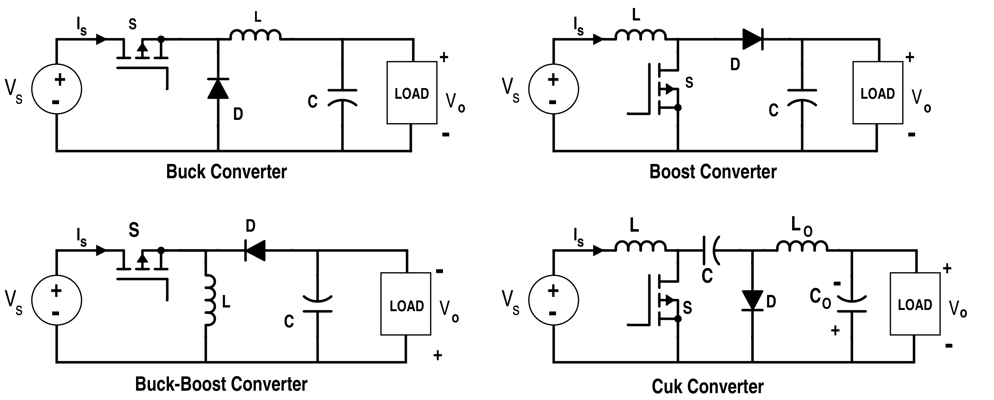
Figure 1. Basic converters
It is worth noticing that any converters work in two distinct modes with respect to the inductor current: the continuous conduction mode (CCM) and discontinuous conduction mode (DCM). When the inductor current is always greater than zero, it is in CCM. When the average inductor current is too low due to the high-load resistance or low-switching frequency, then the converter is in DCM.
The CCM is preferable for high efficiency and efficient use of semiconductor switches and passive components. The DCM requires a special control since the dynamic order of the converter is reduced. Thus, it is required to find out the minimum value of the inductor to maintain the CCM.
Assume that the inductor and capacitor are pure (i.e. no resistive component). However, there is still what we call a small-ripple approximation. In an efficient converter, the output voltage ripple is small. It is assumed that the load is resistive and the DC component of the output voltage has no ripples, or simply the DC output has a fixed value as shown in Fig.2 for making the analysis easier.
So,
∆VO = 0 and VO = V.
.png)
Figure 2. Small-ripple approximation
Buck Converter
.png)
Figure 3. Buck converter circuit diagram
As shown in Fig. 3, the buck converter consists of a DC supply or a rectified AC output, two switches i.e. D (diode) and S (can be semi-controlled or fully-controlled power electronics switches), two-pole low-pass filter (L and C) and a load. Let the duty ratio of switch S be
$$D\,=\,\frac{T_{ON}}{T}$$
where
T=TON+TOFF.
Buck converter is mostly used for DC drives systems e.g. electric vehicles, electric traction and machine tools.
This circuit can be studied in two different modes. The first mode is when the switch S is on while the second mode is when the switch S is off. The circuit diagrams when the switch S is on and off are given in Fig. 4 and Fig. 5 respectively.
$$Voltage\,across\,the\,Inductor\,=\,V_{L} \,=\,L\frac{dI}{dt}$$ where I=IC+IO.
$$Load\,Current\,=\,I_{O}=\frac{V_{O}}{R}$$
.png)
Figure 4. Buck converter circuit when switch S is on (Mode-I)
When the switch S is on and applying the Kirchhoff‘s voltage law (KVL), we can get,
$$V_{S}=V_{L}+V_{O}$$
$$\Rightarrow V_{S}\,=\,L\frac{di}{dt} + V_{O}\;\;and\;\;V_{O}=V_{C}.$$
.png)
Figure 5. Buck converter circuit when switch S is off (Mode-II)
When the switch S is off, the KVL in Fig.5 gives,
$$V_{L} + V_{O} = 0 $$
$$\Rightarrow V_{O}\,=\,-L\frac{di}{dt}.$$
As the output voltage is assumed constant by the small-ripple approximation,
$$\Rightarrow L\frac{di}{dt}\,=\,constant$$
$$\Rightarrow \frac{di}{dt}\,=\,constant$$
$$\Rightarrow slope \,of\,the\, inductor \,current\, is\, constant.$$
Waveforms of the voltage and current during the one-cycle period are shown in Fig. 6.
.png)
Figure 6. Supply current Is, diode current ID, inductor current I, and inductor voltage VL waveforms respectively (buck converter)
As
$$V_{L}=L\frac{di}{dt},$$
$$\Rightarrow (I_{max}-I_{min})_{SWITCH-ON}\,=\,\frac{V_{S}-V_{O}}{L}DT$$ [Equation 1]
and
$$(I_{min}-I_{max})_{SWITCH-OFF}\,=\,-\frac{V_{O}}{L}(1-DT)$$
$$\Rightarrow Average\, Inductor\, Current=\frac{I_{max}+I_{min}}{2}=I$$
From Fig. 6 and from the steady-state perspective, magnitude of the inductor current increment during switch on is equal to the inductor current decrement during switch off; i.e. $$\left | (I_{max}-I_{min})_{SWITCH-ON} \right |=\left| (I_{max}-I_{min})_{SWITCH-OFF}\right|.$$
$$\Rightarrow |\frac{V_{S}-V_{O}}{L}DT|\,=\,|-\frac{V_{O}}{L}(1-DT)|$$
$$\Rightarrow V_{O}\,=\,DV_{S}$$
In the case of the buck converter, output voltage is directly dependent on the duty cycle and the input voltage.
Alternatively, this can also be derived as follows:
As the net inductor current is nil i.e. $$I(T)-I(0)=0;$$
$$\Rightarrow \frac{1}{L}\int_{0}^{T}V_{L}dt=0;$$
$$\Rightarrow$$ Area under the inductor voltage and time is zero. This is called the inductor volt-sec balance for the one cycle of voltage with respect to time under steady-state condition.
$$\Rightarrow (V_{S}-V_{O}) DT\,-\, V_{O}(1-DT)=0$$
$$\Rightarrow V_{O}=DV_{s}$$ [Equation 2]
Now, the average capacitor current is zero for the complete cycle due to the capacitor charge balance.
We know that
$$I_{C}\,=\,C\frac{dv}{dt};$$
For a steady-state condition, net change in the capacitor voltage must be nil.
By integrating the above equation for a complete cycle, we can get,
$$V_{C}(T)\,-\,V_{C}(0)\,=\,\int_{0}^{T}\frac{I_{C}}{C}dt=0;$$
Hence, the total area under the capacitor current and time curve must be zero. This implies that for a complete cycle, average capacitor current IC=0;
$$\Rightarrow I_{O}\,=\,\frac{V_{O}}{R}\,=\,I+I_{C}=I{;}$$
$$\Rightarrow I\,=\,I_{O}\,=\,\frac{V_{O}}{R}\,=\,\frac{I_{max}+I_{min}}{2}$$ [Equation 3]
From Equations 1 and 3, we can get,
$$I_{max}\,=\,DV_{S}(\frac{1}{R}\,+\,\frac{1-D}{2L}T){;}$$ [Equation 4]
and
$$I_{min}\,=\,DV_{S}(\frac{1}{R}\,-\,\frac{1-D}{2L}T){;}$$ [Equation 5]
The capacitor current is alternating for the continuous inductor current as given in Fig. 7.
.png)
Figure 7. Capacitor current
The ripple voltage in the capacitor which depends on the area under the current-time curve is obtained. The charge accumulated during the half cycle is equal to the area under the curve for the capacitor current and time.
$$\Rightarrow ∆Q\,=\,\frac{1}{2}\frac{(I_{max}-I_{min})}{2}(\frac{T}{2})$$
$$\Rightarrow P_{k}\,-\,P_{k} output \,voltage \,ripple\,=\, ∆V_{C}\,=\,\frac{∆Q}{C}\,=\,\frac{D(1-D)V_{S}}{8CL}T^{2}$$ [Equation 6]
Boost Converter
The circuit diagram of the boost converter is shown in Fig. 8. One of the applications of the boost converter is for radar or ignition systems.
.png)
Figure 8. Boost converter circuit diagram
The equivalent circuit during switch on and off condition of the switch S is shown in Fig. 9 and Fig. 10 respectively.
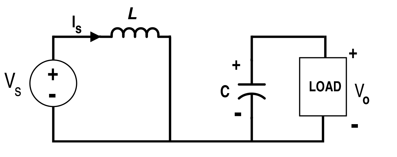
Figure 9. Boost converter circuit when switch S is on (Mode-I)
.png)
Figure 10. Boost converter circuit when switch S is off (Mode-II)
When the switch S is on,
VS=VL
$$\Rightarrow L\frac{di}{dt}\,=\,V_{S}\,=\,Constant \,supply \,voltage$$
$$\frac{di}{dt}=constant$$
$$\Rightarrow Current \,increases\, with\, constant\, slope.$$
When the switch S is off,
$$\Rightarrow V_{S}\,=\,V_{L}\,+\,V_{C}$$
$$\Rightarrow L\frac{di}{dt}\,=\,V_{S}\,-\,V_{C};$$
$$\Rightarrow \frac{di}{dt}\,=\,\frac{(V_{S}-V_{C})}{L}.$$
Now, current decreases and must reach at a value equal to the value of the current at the initial stage when switch S is just switched on according to steady-state stability.
Current increment during switch on
$$=\,I_{max}\,-\,I_{min}\,=\,\frac{V_{S}}{L}DT$$ [Equation 7]
Current decrement during switch off
$$= \,I_{min}\,-\,I_{max}\,=\,\frac{V_{S}\,-\,V_{C}}{L}(1-D)T$$ [Equation 8]
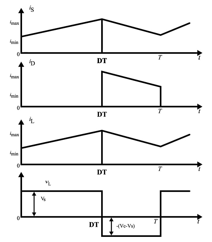
Figure 11. Supply current, diode current, inductor current, and inductor voltage respectively (boost converter)
According to the inductor volt-sec balance,
$$V_{S}.DT=(V_{S}-V_{C}).(1-D)T$$
$$\Rightarrow V_{C}=\frac{V_{S}}{1-D}$$
$$\Rightarrow V_{O}=\frac{V_{S}}{1-D}$$ [Equation 9]
$$Average\,Inductor\,Current = \frac{I_{max}+I_{min}}{2}$$
$$Input\,Power,\,P_{IN}=\frac{I_{max}+I_{min}}{2}V_{S}$$
$$Output\,Power,\,P_{OUT}=\frac{V_{O}^{2}}{R}=\frac{V_{S}^{2}}{(1-D)^{2}R}$$ (from Equation 9) [Equation 10]
Assume there is no switching loss,
$$\Rightarrow P_{IN}=P_{OUT}$$
$$\Rightarrow I_{max}+I_{min}\,=\,2\frac{V_{S}}{R(1-D)^{2}}$$ [Equation 11]
From Equations 11 and 8, we can get,
$$I_{min}\,=\,\frac{V_{S}}{R{(1-D)}^{2}}-\frac{V_{S}}{2L}DT$$ [Equation 12]
$$I_{max}=\frac{V_{S}}{R(1-D)^{2}}+\frac{V_{S}}{2L}DT$$ [Equation 13]
For the continuous conduction mode (CCM), $$I_{min}=0;$$
$$\Rightarrow L_{min}=\frac{D(1-D)^{2}}{2}TR$$ [Equation 14]
Ripple voltage across the capacitor
$$ = ∆V_{C}=\frac{∆Q}{C}$$
Where, ∆ Q is the charge accumulated during the switch-on condition.
$$\Rightarrow ∆V_{C}={DT}\frac{V_{O}}{R}.\frac{1}{C}$$
$$\Rightarrow ∆V_{C}=\frac{DTV_{S}}{(1-D)RC}$$ [Equation 15]
Buck-Boost Converter
This converter is an inverting DC-to-DC converter i.e. polarity of the output voltage is reversed compared to the input supply. Thus, it is a negative-output buck-boost converter.
.png)
Figure 12. Buck-boost converter circuit diagram
Let the capacitor be totally charged up before switching on the switch S. When the switch S is closed as shown in Fig. 13,
-VS + VL = 0
$$\Rightarrow V_{S}=V_{L}=L\frac{di}{dt}$$
.png)
Figure 13. Buck-boost converter circuit when switch S is on (Mode-I)
Also,
-VC + VO = 0
$$\Rightarrow V_{O}=V_{C}$$
.png)
Figure 14. Boost converter circuit when switch S is off (Mode-II)
Now, when the switch S is opened as given in Fig. 14,
+VL + VC = 0
$$L\frac{di}{dt}+V_{C}=0$$
$$\frac{di}{dt}=-\frac{V_{C}}{L}$$
Waveforms for the voltage and current for buck-boost converter are shown in Fig. 15.
.png)
Figure 15. Supply current, diode current, inductor current, and inductor voltage respectively (buck-boost converter)
Now, from the waveforms given in Fig.15,
When switch S is on,
$$Rise\,in\,the\,Inductor\,Current = I_{max}-I_{min}=\frac{V_{S}}{L}DT$$ [Equation 16]
And, when switch S is off,
$$ Fall\,in\,the\,Inductor\,Current = I_{min}-I_{max}=-\frac{V_{C}}{L}(1-D)T$$ [Equation 17]
Equating the Equations 16 and 17, we can get,
$$\frac{V_{S}}{L}DT=\frac{V_{C}}{L}(1-D)T$$
$$\Rightarrow V_{O}=V_{C}=\frac{D}{1-D}V_{S}$$ [Equation 18]
$$Average\,Inductor\,Current = \frac{I_{min}+I_{max}}{2}$$
As there is no supply current during the switch-off condition,
$$Input\,Power = P_{IN}=\frac{I_{max}+I_{min}}{2}DV_{S}$$
And,
$$Output\,Power = P_{OUT}=\frac{{V_{O}}^{2}}{R}$$
If there is no switching loss,
PIN=POUT
$$\Rightarrow I_{max}+I_{min}=2D\frac{V_{S}}{R(1-D)^{2}}$$ [Equation 19]
From Equations 17 and 19, we can get,
$$I_{min}=D\frac{V_{S}}{R(1-D)^{2}}-\frac{V_{S}}{2L}D$$ [Equation 20]
and
$$I_{max}=D\frac{V_{S}}{R(1-D)^{2}}+\frac{V_{S}}{2L}DT$$ [Equation 21]
For CCM, Imin=0
$$\Rightarrow Value\,of\,the\,Minimum\,Inductance\,for\,CCM=
L_{min}=\frac{{(1-D)}^{2}}{2}TR$$
$$Ripple\,Voltage\,Across\,the\,Capacitor =
∆V_{C}=\frac{∆Q}{C}=\frac{DTI_{O}}{C}=\frac{DTV_{O}}{RC}=\frac{{D}^{2}TV_{S}}{(1-D)RC}$$
as
$$V_{O}=\frac{D}{(1-D)}V_{S}$$
Note:
When D < 0.5, it acts as a step-down converter or a buck converter.
When D > 0.5, it acts as a step-up converter or a boost converter.
And when D = 0.5, input and output voltages are the same i.e.VO=VS.
That is why buck-boost converters are also called as DC transformers due to the same role in the case in AC.
The converter discussed above is a negative-output buck-boost converter. But in some applications, reversal of polarity is not allowed. In such cases, we require a positive-output converter whose configuration diagram is given below:
.png)
Figure 16. Positive-output buck-boost converter circuit diagram
Ćuk Converter
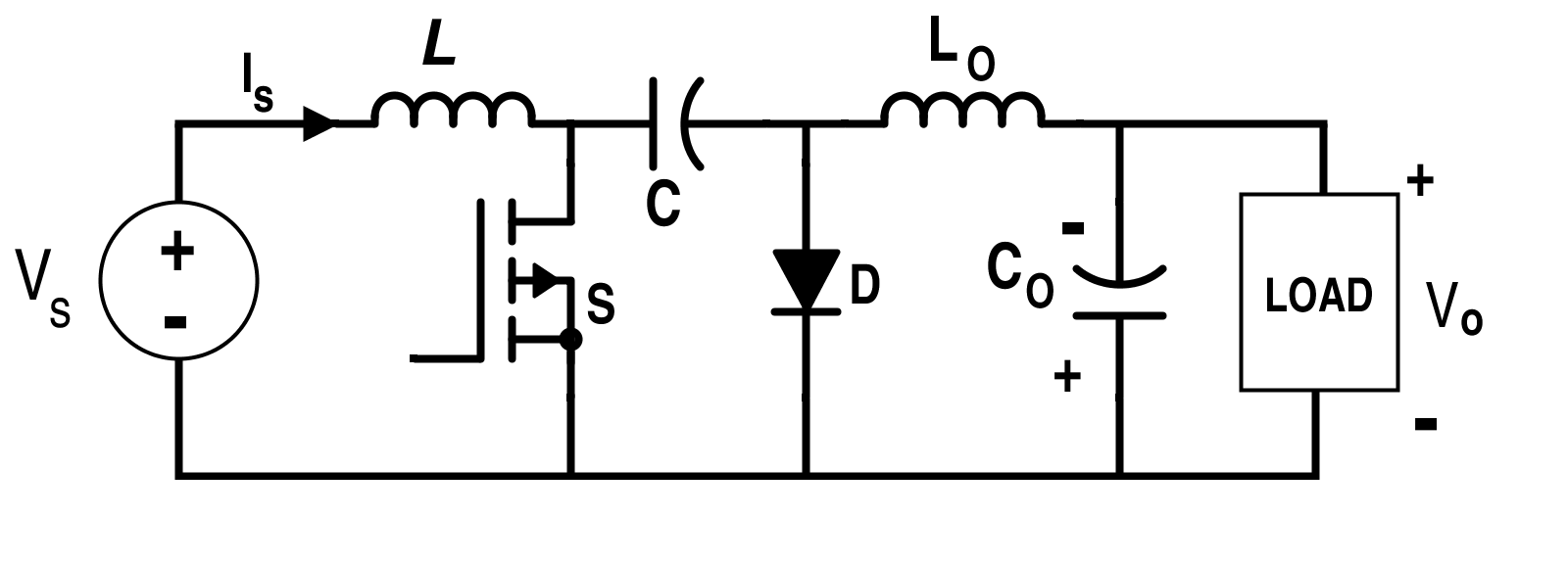
Figure 17. Ćuk converter circuit diagram
A Ćuk converter can be obtained by cascading the boost converter followed by the buck converter. It also has a negative-output polarity as in the case of the simple buck-boost converter. But we have assumed here that the polarity of the output is positive.
.png)
Figure 18. Ćuk converter circuit when switch S is on (Mode-I)
When switch S is on, the circuit will be reduced as shown in Fig. 18.
From Fig.18,
VS=VL
$$\Rightarrow \frac{di}{dt}=\frac{V_{S}}{L}$$ (Current Increases)
$$\Rightarrow ∆I_{L}=V_{S}.\frac{DT}{L}$$ [Equation 22]
For inductor LO,
VC+VLo+VO=0
$$\Rightarrow \frac{dI_{Lo}}{dt}=-\frac{1}{L}(V_{C}+V_{O})$$ (Current Increases)
If the VC and VCO polarities are in the reverse direction of the loop considered and the current must increase, the current must actually increase in the opposite direction of the assumed direction.
.png)
Figure 19. Ćuk converter circuit when switch S is off (Mode-II)
When switch S is off, the circuit will reduced to the configuration shown in Fig.19.
From Fig. 19,
-VS+VL+VC=0
$$\Rightarrow \frac{di}{dt}=\frac{-(V_{C}-V_{S})}{L} $$ (Current decreases)
For inductor Lo,
VLo-VCo=0
$$\Rightarrow \frac{dI_{Lo}}{dt}=\frac{V_{Co}}{L}$$ (Current decreases)
Note that the current actually decreases in the opposite direction. So, $$\frac{di}{dt}$$ must be positive.
Also, from the Figure 19, it is clear that capacitor C is charging up for the time (1-D).T.
$$\Rightarrow ∆V_{C}=\frac{∆Q}{C}=\frac{1}{C}\int_{0}^{(1-D)T}I_{C}dt=I_{S}\frac{(1-D)T}{C} $$ [Equation 23]
(As IC=IS from Fig.19)
By volt-sec balance,
$$V_{S}.DT=(V_{C}-V_{S}).(1-D)T$$
$$\Rightarrow V_{C}=\frac{1}{(1-D)}V_{S}$$ [Equation 24]
And, $$(V_{C}+V_{Co})DT=-V_{Co}(1-D)T$$
$$\Rightarrow V_{C}D=-V_{Co}$$
From Equation 23,
$$\Rightarrow V_{Co}=-\frac{D}{1-D}V_{S}$$
Also, VO=-VCo
$$V_{O}=\frac{D}{(1-D)}V_{S}$$ [Equation 25]
From the capacitor charge balance condition and from the Fig. 19,
IL=IS and ILo=IO
Now, assume there is no switching loss within the converter,
PIN = VS IS
POUT = VO IO
$$\Rightarrow V_{S}I_{S}=\frac{D}{1-D}V_{S}I_{O}$$
$$\Rightarrow I_{S}=\frac{D}{(1-D)}I_{O}$$ [Equation 26]
Where $$I_{O} =\frac{ V_{O}}{ R}$$
According to the small-ripple approximation, ripples due to load itself are negligible. So,∆ICo=∆ILo.
.png)
Figure 20. Switch (S) voltage, capacitor (C) voltage, inductor (L) current, inductor (LO) current, capacitor (CO) voltage, capacitor (C) current, and load current respectively for the Ćuk converter
From Fig. 20, average charging current for CO which flows for $$\frac{T}{2}$$ duration $$=\frac{∆I_{Lo}}{4}.$$ It is also shown in Fig. 21. Thus, ripple voltage across the capacitor CO is given by
$$∆V_{Co}=\frac{1}{Co}\int_{0}^{\frac{T}{2}}I_{Co} dt=\frac{1}{Co}\int_{0}^{\frac{T}{2}}\frac{∆I_{Lo}}{4} dt =\frac{∆I_{Lo}}{8Co}T$$ [Equation 27]
.png)
Figure 21. Inductor (LO) current and capacitor (CO) voltage
As, $$∆I_{Lo}=\frac{V_{O}(1-D)T}{L_{Lo}}$$
$$∆V_{Co}=D\frac{V_{S}}{8Co L_{Lo}} T^{2}$$ [Equation 28]
.png)
Figure 22. Inductor( L) current
From Fig. 22, it is clear that for continuous inductor current i.e. for CCM, $$∆I_{L}=2I_{Lavg}= 2I_{S},$$ where ILavg is the average current through inductor L.
(Due to capacitor charge balance, IS=ILavg)
From Equations 26 and 22,
$$D\frac{V_{S}T}{L}=∆I_{L}=2I_{S}=2\frac{D}{1-D}I_{O}=2{(\frac{D}{1-D})}^{2}(\frac{V_{S}}{R})$$
$$\Rightarrow L_{min}=\frac{(1-D)^{2}R}{2D}T$$
Similarly, from Fig. 20, for CCM
$$∆I_{Lo}=2I_{Loavg}=2 I_{O}=2\frac{V_{O}}{R}$$
Where ILoavg is the average current through the inductor LO.
As,
$$∆I_{Lo}=DV_{S}\frac{T}{L_{Lo}}$$
$$\Rightarrow L_{Lo_{min}}=\frac{(1-D)RT}{2}$$
If VC is the capacitor average voltage across C, the CCM from Fig. 20,
Capacitor (C) Ripple Voltage = ∆VC = 2 VO = 2 IO R
From Equation 23,
$$\Rightarrow \frac{I_{S}(1-D)T}{C}=2I_{O}R$$
$$C_{min}=\frac{DT}{2R}$$
In the CCM from Fig. 18, if VCo is the capacitor average voltage across CO,
Capacitor CO Ripple Voltage = ∆VCo = 2 VO = 2 IO R
From Equation 28,
$$\Rightarrow D\frac{V_{S}}{8C_{O}L_{O}}T^{2}=2V_{O}=2\frac{D}{1-D}V_{S}$$
$$\Rightarrow Co_{min}=\frac{1}{8R}T$$
The main benefit of the Ćuk converter is that you can control the continuous current at both in the input and output of the converter as it is based on the capacitor energy transfer. It has a low-switching loss making it more highly efficient. The downside of this converter is that it includes a high number of reactive components (L and C) and heavy current stresses on the components. And since the capacitor C provides a transfer of energy, ripples in the capacitor (C) current are high.


Great article. Thank so lot.
Thanks interesting article. I noticed a few typos in the equations:
After $$Equation\;1.$$ the SWITCH-OFF current delta should be: $$(I_{min}-I_{max})_{SWITCH-OFF}\,=\,-\frac{V_{O}}{L}(1-D)T$$
For the boost converter the voltage-sec balance before $Equation\;9.$ should be: $$V_{S}DT=-(V_{S}-V_{C})(1-D)T$$
Also I would like to better understand how we get the buck converter ripple voltage. In Figure 7. we have increasing capacitor current until $DT$ then decreasing current until $$T$$, but the following integration is done for the $$\frac{T}{2}$$ period. How do the two periods $$DT$$ and $$\frac{T}{2}$$ relate to each other? How does the ripple voltage-time curve look like, does it consist of a $$0..\frac{T}{2}$$ and a $$\frac{T}{2}..T$$ symmetric periods or a $$0..DT$$ and a $$DT..T$$ (asymmetric) period?
Thanks
thanks alot.