 Facebook
 Google
 GitHub
 Linkedin
Error Analysis in Analog-to-digital Converter (ADC) Applications
Through four different examples, learn about analog-to-digital converter (ADC) system error analysis.
When designing a measurement system, we need to fully understand different sources of error and how they contribute to the overall accuracy. An error analysis allows us to choose our components confidently and ensure that the system meets the accuracy requirements.
This article delves into a discussion on ADC system error analysis through different examples.
Typical Errors in a Signal Chain
Figure 1 shows a block diagram for resistive current sensing application.
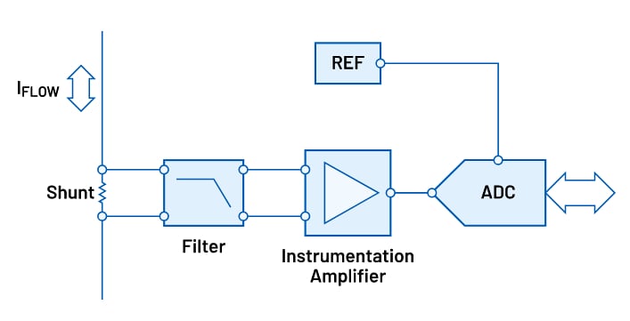
Figure 1. A block diagram for a resistive current sensing application. Image used courtesy of Analog Devices
Although the ADC is a key component, it’s only one source of error in the measurement system. There might be several other components, such as filters, amplifiers, the ADC input driver, and voltage reference, that add extra error to the system. The non-idealities of these components manifest themselves as an increase in the overall offset error, gain error, or nonlinearity of the system. Depending on the application and circuit topology, the errors from a particular component might be more significant than others.
ADC Gain Error Depends on Signal Level
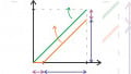
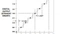
Before proceeding, we need to highlight an important difference between the gain and offset errors: unlike the offset error, the gain error depends on the signal level. To better understand this, consider the characteristic curve of the 3-bit ADC depicted below (Figure 2), which has an offset error of -1.5 LSBs (least significant bit).
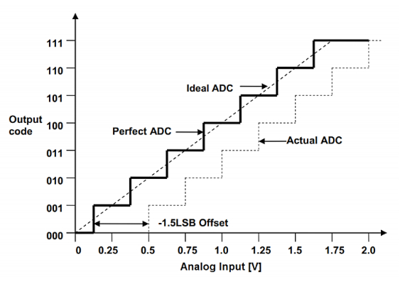
Figure 2. Example 3-bit ADC characteristic curve with a -1.5 LSB offset error. Image used courtesy of Microchip
Note that an offset error shifts the entire transfer function by the same value. In other words, it introduces the same error value no matter what the input signal level is. However, this is not the case for a gain error. The following diagram of Figure 3 shows a 3-bit ADC with +1.5 LSBs of gain error.
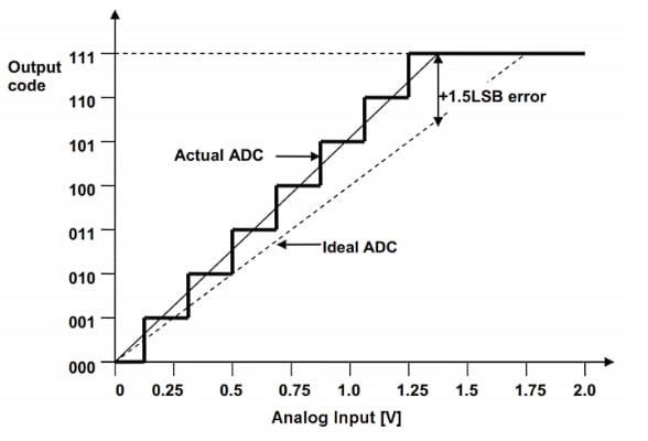
Figure 3. Example 3-bit ADC plot with a +1.5 LSB gain error. Image used courtesy of Microchip
For an input signal at the upper end of the input range (about 1.4 V), the gain error is +1.5 LSBs; however, at the lower end of the input range, the error is zero. For an input at the midpoint of the range, the gain error is about +0.75 LSBs. Therefore, the gain error scales with the input signal. This means that if, in a particular application, the input level is always smaller than the full-scale value, the effective gain error is only a portion of the rated value. Let’s look at an example.
Example 1: Applying TUE and Monitoring a Power Supply
Assume that we must monitor a 1 V power supply for any out-of-tolerance condition. What would be the total unadjusted error (TUE) of our measurement if we used a 12-bit ADC with a reference voltage of 3 V and the following error values, shown in Table 1?
Table 1. ADC Error Values
|
Error |
Value (LSBs) |
|
Integral Nonlinearity (INL) |
3 |
|
Offset Error |
2.5 |
|
Gain Error |
4 |
Assuming that the input has only small variations about its nominal value of 1 V, we can calculate the effective gain error as follows:
\[E_{gain}=\frac{V_{in}}{V_{ref}}\times Gain \text{ } Error=\frac{1}{3} \times 4=1.33 \text{ }LSBs\]
Substituting this value in the TUE equation, we can estimate the total error using Equation 1.
\[TUE=\sqrt{(Offset \text{ } Error)^2+(E_{gain})^2+ INL^2}=\sqrt{2.5^2+1.33^2+3^2}=4.13 \text{ } LSBs\]
Equation 1.
This is equivalent to a loss of log2(4.13) = 2.05 bits of accuracy. Without taking the input signal level into account, we would have estimated the TUE to be 5.6 LSBs.
ADC Voltage Reference Effect
In the above example, we only considered the ADC errors. How can we take the voltage reference errors into account? The voltage reference determines the full-scale value of the ADC. We know that we can model the ADC transfer function by the following straight-line equation in Equation 2.
\[Code = \frac{V_{in}}{V_{Ref}} \times 2^{N}\]
Equation 2.
Where:
- Vin is the input voltage
- VRef denotes the reference voltage (or the full-scale voltage)
- N is the number of bits
Suppose that the actual value of VRef is slightly different from its ideal value and is given by:
\[V_{Ref,\text{ }m}=V_{Ref}(1+\alpha)\]
Where α is a small value denoting the reference error. Therefore, Equation 2 can be rewritten as:
\[Code = \frac{V_{in}}{V_{Ref}(1+\alpha)} \times 2^{N}\]
Using the Taylor series concept, we can approximate $$ \frac{1}{1+ \alpha}$$ with $$1- \alpha$$. Therefore, we obtain:
\[Code = \frac{V_{in}}{V_{Ref}} \times 2^{N} \times (1-\alpha)\]
Comparing this with the ideal relationship in Equation 2, we can observe that a small error in VRef leads to approximately the same error in the slope of the transfer function. For example, if the initial accuracy of the voltage reference is 0.05%, the ADC gain is 0.05% different from its ideal value. In this case, we’ll have a gain error of 0.05% only due to the voltage reference inaccuracy. Example 2 further clarifies how the voltage reference error can be calculated.
Example 2: Monitoring a Power Supply With a Non-ideal Reference
A voltage reference should ideally produce a constant voltage independent of the electrical and environmental conditions of the application. However, the output of a real-world voltage reference changes with factors such as temperature, time (known as long-term stability), power supply, load current, and thermal hysteresis. Also, just like any other electronic component, voltage references produce some noise that increases the signal-to-noise ratio (SNR) of the system.
One thing you might wonder is, how are all these non-idealities going to affect the accuracy of our measurements? To answer that, let's assume that the voltage reference for the above example has the following specifications, shown in Table 2.
Table 2. Errors and Values for Example 2.
|
Error |
Value |
|
Initial Accuracy (Einit) |
0.05% |
|
Temperature Drift |
10 ppm/°C |
|
Line Regulation |
50 ppm/V |
|
Thermal Hysteresis (Ehys) |
40 ppm |
|
Long-Term Stability (ELTD) |
35 ppm |
|
1/f noise |
30 µVp-p |
Assuming that the power supply of the voltage reference can have a total variation of 1 V, we get the following equation for the line regulation error:
\[E_{line}= Line \text{ } Regulation \times \Delta V_{in}=50 \times 1=50 \text{ }ppm\]
Since other error terms are in ppm, the noise value should be expressed in ppm as well:
\[E_{noise}= \frac{Noise}{V_{Ref}} \times 10^{6}=\frac{30 \text{ } \mu V_{p-p}}{3 \text{ }V} \times 10^{6}= 10\text{ }ppm\]
The root-sum-square (RSS) equation can now be applied to estimate the total error from the voltage reference:
\[E_{Reference}=\sqrt{(E_{init})^2+(E_{temp})^2+ (E_{line})^2+(E_{hys})^2+(E_{LTD})^2+(E_{noise})^2}\]
Substituting the error terms, we obtain:
\[E_{Reference}=\sqrt{500^2+700^2+ 50^2+40^2+35^2+10^2}=863.4 \text{ }ppm\]
Since the voltage reference error leads to a gain error in the ADC system; and noting that the ADC input is only one-third of the full-scale value, we can calculate the effective gain error as:
\[E_{R}=\frac{1}{3} \times 863.4 =287.8 \text{ }ppm\]
In a 12-bit system, this value is equal to 1.18 LSBs, as calculated below (Equation 3):
\[E_{R, \text{ } LSB}=E_R \times 2^{12}=287.8 \times 2^{12}=1.18 \text{ }LSBs\]
Equation 3.
Finally, the system error is found by applying the RSS equation to the values obtained from Equations 1 and 3:
\[TUE=\sqrt{4.13^2+1.18^2}=4.3 \text{ } LSBs\]
To learn more about voltage reference errors, you can refer to “Voltage Reference Selection Basics” and “Calculating the Error Budget in Precision Digital-to-Analog Converter (DAC) Applications.”
Example 3: A 3-wire RTD Measurement System
As mentioned above, the application and sensor type determines the circuit topology and, thus, the type and significance of different error sources. As an example, consider the 3-wire resistance temperature detector (RTD) system below in Figure 4.
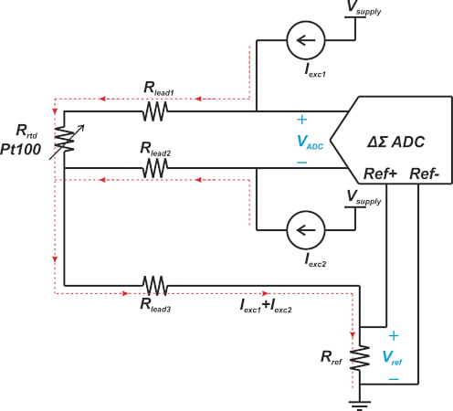
Figure 4. Example 3-wire RTD system diagram.
For this example, in addition to the ADC error terms, the tolerance of the reference resistor Rref and the mismatch of the excitation currents (Iexc1 and Iexc2) introduce errors in our measurement. Since Rref determines the reference voltage of the ADC, its tolerance produces a gain error in the ADC transfer function. Considering our previous discussion on the effect of the voltage reference error, we can conclude that a given error in Rref leads to the same gain error in the ADC transfer function. For example, if the tolerance of Rref is 0.02%, the gain error from the reference voltage inaccuracy is about 0.02%.
In RTD applications, we need identical excitation currents to eliminate the RTD lead resistance error. That brings to mind the question of how is a mismatch in the current sources going to affect the system's accuracy? To answer this question, we need to examine the transfer function of the system. The ADC input voltage is calculated as:
\[V_{ADC}=R_{lead1}I_{exc1}+R_{rtd}I_{exc1}-R_{lead2}I_{exc2}\]
Assume that Iexc2 = Iexc1(1 + α), where α denotes the mismatch in the excitation currents. For identical lead resistances (Rlead1 = Rlead2), we can rewrite the above equation as Equation 4 below.
\[V_{ADC}=\big ( R_{rtd}-R_{lead1}\alpha \big)I_{exc1}\]
Equation 4.
Noting that the sum of the excitation currents flows through Rref, Equations 2 and 4 yields the output code as:
\[Code = \frac{\big ( R_{rtd}-R_{lead1}\alpha \big)}{R_{Ref}\big(2+\alpha \big)} \times 2^{N}\]
For simplicity, let’s assume that Rlead1α ≪ Rrtd. Therefore, the transfer function simplifies to:
\[Code = \frac{R_{rtd}}{R_{Ref}\big(2+\alpha \big)} \times 2^{N}\]
Again, using the Taylor series concept, we can approximate $$\frac{1}{2+ \alpha}$$ as:
\[\frac{1}{2+\alpha}=\frac{1}{2}\times\frac{1}{1+\frac{\alpha}{2}} \approx \frac{1}{2}(1-\frac{\alpha}{2})\]
Therefore, the output code can be calculated by Equation 5:
\[Code = \frac{R_{rtd}}{R_{Ref}} \times 2^{N} \times \frac{1}{2}(1-\frac{\alpha}{2})\]
Equation 5.
By substituting α = 0, the ideal response is found in Equation 6:
\[Code = \frac{R_{rtd}}{R_{Ref}} \times 2^{N} \times \frac{1}{2}\]
Equation 6.
Comparing Equations 5 and 6, we observe that a mismatch of α in excitation currents produces a gain error of about $$\frac{\alpha}{2}$$ in the system response. For example, if the current mismatch is 0.15% (or α = 0.0015), the gain error is about 750 ppm. You can find alternative proof of this derivation in this TI document.
Example 4: A Thermocouple Measurement System
As the final example in this article, let’s take a look at the thermocouple application depicted in Figure 5.
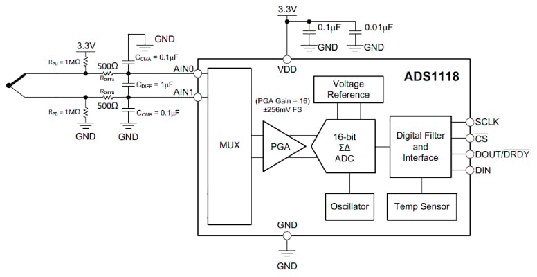
Figure 5. Example thermocouple application block diagram. Image used courtesy of TI
For this example, in addition to the ADC and voltage reference error terms, the filter resistors can also contribute to the system error if the input impedance of the ADC is relatively low. The total series resistance from the filter is 1000 Ω. This resistance interacts with the differential input impedance of the ADC and attenuates the thermocouple signal. For example, the ADS1118 exhibits a differential input impedance of 710 kΩ. Therefore, the ADC input signal is calculated as:
\[V_{ADC}=\frac{R_{in}}{R_{in}+R_{filter}}V_{Thermocouple}=\frac{710}{710+1}V_{Thermocouple}=0.9986\times V_{Thermocouple}\]
Ideally, we expected the thermocouple signal to appear at the ADC input with no attenuation (gain = 1). Therefore, the filter resistance introduces a gain error of about 0.14%. The gain error from the filter can be negligible if the input impedance of the ADC is sufficiently larger than the filter resistance. It’s worthwhile to mention that when performing error analysis, one might also need to take into account the temperature drift of error terms, such as the gain and offset drift of the ADC.
Featured image used courtesy of Adobe Stock
To see a complete list of my articles, please visit this page.


Many thanks for the Excellent explanation !! please add more such insightful articles in the future
please also include a simple example of error due to resistor tolerance and TCR into ADC error. A simple example could be the output of a resistor voltage divider connected to a ADC.
The link pertaining to temperature drift of error terms is not taking us to the correct webpage or document. please correct it.