Facebook
 Google
 GitHub
 Linkedin
Low-Noise Voltage References: Understanding the Noise Performance of a Voltage Reference IC
Working with a low noise voltage reference? Learn more about noise specifications and relevant voltage reference ICs.
Working with a low noise voltage reference? Learn more about noise specifications and relevant voltage reference ICs.
Many systems such as data converters, power supplies, and measurement and control systems need voltage references to produce a stable voltage. The accuracy of these systems will be directly affected by the accuracy of the produced reference voltage.
In a previous article on the temperature coefficient of voltage references, we saw that the tempco specification can be used to determine the maximum temperature-induced error in the output of a voltage reference.
In this article, we’ll take a look at the noise specification of a voltage reference.
Why Is Reference Noise Important?
As an example, let’s consider using a voltage reference to set the full-scale value of a three-bit ADC. The full-scale value represents the range of voltages the ADC is capable of encoding.
The transfer characteristic of a three-bit ADC is shown in Figure 1.
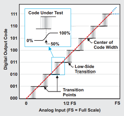
Figure 1. Image courtesy of Texas Instruments.
As you can see, the transition from one digital code to the next does not occur at exactly one value of the analog input—there’s a small region of uncertainty. In other words, if we measure the transition point from one code to the next several times, we won’t get a single threshold value for the analog input. Remember that an ADC uses analog comparators to compare the analog input with a known voltage created from the reference voltage. The noise generated by the different components within the ADC structure leads to the transition noise depicted in Figure 1.
Similarly, the noise on the reference voltage can affect the output of the analog comparators. Hence, a noisy voltage reference can further increase the transition noise. The transition noise will increase the noise level at the converter output to above what we expect from an ideal converter. Therefore, the noise of the voltage reference is an important parameter that directly affects the signal to noise ratio (SNR) of the overall system.
If you'd like to learn more about reference noise in relation to ADCs, check out How Voltage Reference Noise Affects Delta Sigma ADCs from the series by Texas Instruments.
Noise Specifications for a Reference
Some manufacturers specify the noise of a voltage reference as a peak-to-peak value in the 1/ƒ region (usually ranging from 0.1 Hz to 10 Hz). Some others characterize the wideband RMS noise over a specified frequency range (for example, from 10 Hz to 1 KHz).
The most useful way is to provide the plot of the noise voltage spectral density ($$nV/\sqrt{Hz}$$) versus frequency (as seen in Figure 2 below). Note the 1/ƒ and broadband noise regions shown in Figure 2.
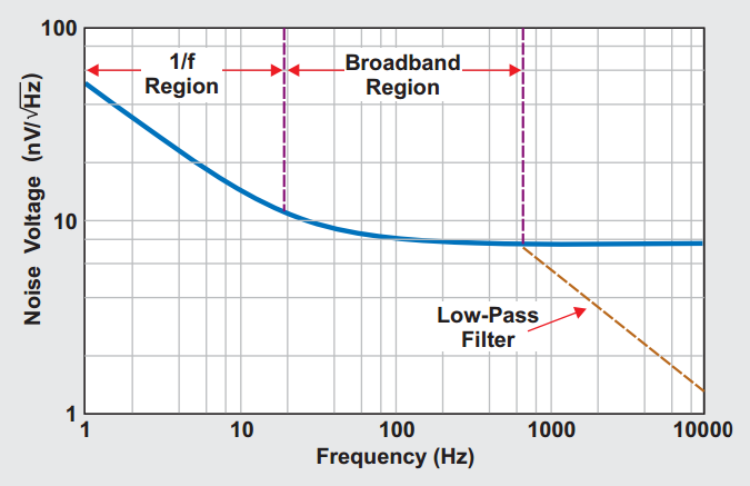
Figure 2. Image courtesy of Texas Instruments.
We can employ a low-pass filter at the output of a voltage reference to suppress its noise significantly. Suppressing the broadband noise is relatively easier compared to suppressing the 1/ƒ noise because for the 1/ƒ region, we need a filter with a much lower -3dB bandwidth. The extremely low corner frequency requires large capacitors and resistors. A large capacitor can exhibit a higher leakage current and lead to voltage error and long-term instability.
When assessing the noise performance of a voltage reference, we usually need to convert the peak-to-peak noise to the RMS value and vice versa. To this end, depending on how we define the peak-to-peak value, we can use either of these two formulas 6×Vnoise, rms = Vnoise, p-p or 6.6×Vnoise, rms = Vnoise, p-p. Please see this video from Analog Devices for more details.
We may also need to convert the noise power spectral density ($$nV/\sqrt{Hz}$$) to the RMS value. To do this we multiply the square root of the system bandwidth by the noise spectral density (PSD), i.e. $$V_{noise,rms}=PSD\times \sqrt{BW}$$. Please see this additional ADI video to learn about the assumptions that lead to this equation.
As an example, if the noise spectral density of a voltage reference is $$100nV/\sqrt{Hz}$$ and the bandwidth of the system is limited to 10 kHz (for example by applying a low-pass filter), the noise RMS value will be $$100\frac{nV}{\sqrt{Hz}}\times \sqrt{10,000Hz}=10µV$$. The equivalent peak-to-peak noise will be about 60 µV.
How Much Reference Noise Can We Tolerate?
Let’s assume that we are using a voltage reference to set the full-scale value of an N-bit ADC. How can we determine the required noise spectral density for the voltage reference of this system? In such cases, we can assume that the peak-to-peak value of the noise is less than half the Least Significant Bit or LSB (where $$LSB=\frac{V_{REF}}{2^N}$$):
$$V_{noise, p-p}≤\frac{1}{2}\times \frac{V_{REF}}{2^N}$$
Using the equation mentioned earlier $$6\times V_{noise,rms}=V_{noise,p-p}$$, we obtain:
$$V_{noise, rms}≤\frac{1}{12}\times \frac{V_{REF}}{2^N}$$
Considering the equation $$V_{noise,rms}=PSD\times \sqrt{BW}$$, we arrive at:
$$PSD≤\frac{1}{12}\times \frac{V_{REF}}{2^N\times \sqrt{BW}}$$
For example, assume that we have a 12-bit system with a full-scale value of 5 V and the bandwidth is 100 KHz. Using the above equation, we observe that the voltage reference should have a noise density less than $$322nV/\sqrt{Hz}$$. For a high-resolution system, the above equation may give PSD values that are not easily achievable in practice. In these cases, we’ll have to use some sort of filtering to limit the bandwidth and suppress the noise. The rest of the article takes a look at the techniques of voltage reference noise reduction.
Voltage Reference ICs with Noise Reduction Terminals
Some voltage references have dedicated noise reduction terminals. These terminals can be used to filter the noise of the reference and achieve higher performance. However, it should be noted that each voltage reference in this category may require different circuitry to implement noise filtering. There’s no single solution applicable to all of these voltage references. Hence, before doing anything, one should thoroughly study the device datasheet for any explicit information on this subject.
In this section, we’ll take a look at TI’s REF50xx family that have noise reduction terminals. Figure 3 below shows a simplified block diagram for these voltage references.
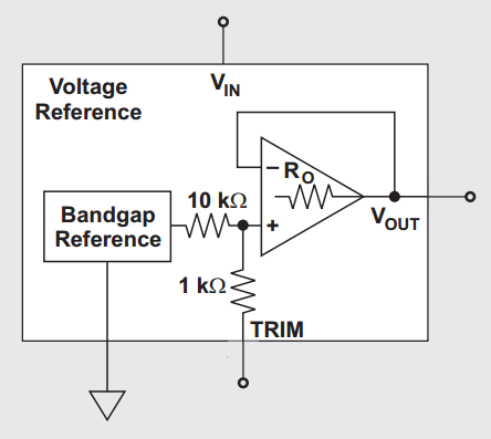
Figure 3. Image courtesy of Texas Instruments.
There are two main noise sources: the bandgap reference and the output buffer/amplifier. As you can see, the TRIM terminal in Figure 3 is connected to the output of the bandgap block. This allows us to connect an external capacitor to the TRIM terminal and create a low-pass filter at the output of the bandgap circuitry.
According to the TI documents, connecting a 1 μF capacitor will reduce the total output RMS noise by a factor of 2.5. Additionally, we can add an external capacitor to the output terminal (VOUT) and create a low-pass filter. Adding these two capacitors, we obtain the schematic shown in Figure 4. This design is suitable for an 8 to 14-bit data converter.
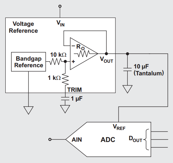
Figure 4. Image courtesy of Texas Instruments.
The equivalent series resistance (ESR) of the 10-μF capacitor is important because this capacitor is directly connected to the output of the internal op-amp that employs a feedback path. With a low ESR (about 0.1 Ω), the feedback system is almost directly connected to a large load capacitor. Driving a large load capacitor can make the op-amp marginally stable and lead to gain peaking. However, according to the TI documents, with an ESR of about 1.5 Ω, we can avoid the stability problem. If you'd like to learn more about large load capacitors, I recommend this video from Analog Devices to learn about why a relatively large ESR can make the system stable.
Note that a larger gain peaking will lead to a larger noise at the reference output (see Figure 5).
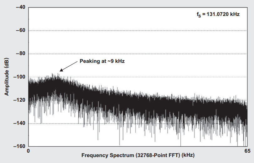
Figure 5. Image courtesy of Texas Instruments.
Considering all these details, we should thoroughly study the datasheet of a voltage reference before applying any filtering technique to suppress the reference noise.
Voltage Reference ICs that Don’t Have Noise Reduction Terminals
For the voltage references that don’t have noise reduction terminals, we can use a precision op-amp to implement a low-pass filter. The schematic is shown in Figure 6.
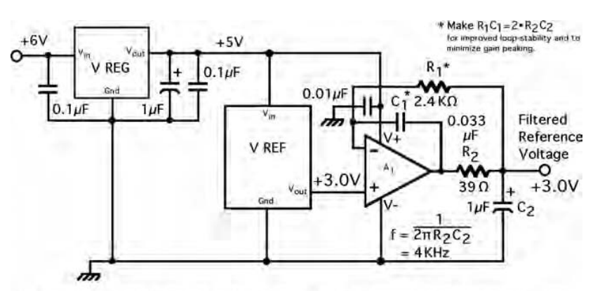
Figure 6. Image courtesy of Current Sources and Voltage References.
As you can see, the single-pole low-pass filter created by R2 and C2 is at the output of the precision amplifier. In this way, we can avoid driving a large capacitive load by the voltage reference IC. While the low-pass filter will suppress the noise coming from both the reference and the op-amp, we still need the op-amp to be very low-noise, low offset, and low drift. The resistors should be low TC precision types and the capacitors should be high-quality polypropylene capacitors.
Note that, as shown in Figure 6, we can use a low-cost, linear voltage regulator to create a clean supply voltage for both the reference and the op-amp. Additionally, choosing R1C1=2R2C2 improves the loop stability of the filter.
The above two techniques are not the only possible solutions for suppressing the noise of a voltage reference. For example, you can replace the above single-pole filter with a much more complicated filter. Please refer to chapter 12 of the book Current Sources and Voltage References to learn about using other types of filters. Besides that, you can find interesting techniques in the manufacturers’ application notes. For example, a Maxim Integrated tutorial explains using a stack of four voltage references to reduce the reference noise by a factor of 2.
Key Points on Noise in Voltage References
- The noise of a voltage reference can directly affect the noise performance of a system. It is usually characterized in two different frequency bands: the 1/ƒ region (from 0.1 Hz to 10 Hz) and the broadband region (for example, from 10 Hz to 1 KHz).
- We can employ a low-pass filter at the output of a voltage reference to suppress its noise significantly. Suppressing the broadband noise is relatively easier compared to suppressing the 1/ƒ noise.
- We usually assume that the peak-to-peak value of the noise generated by the voltage reference is less than half the LSB of the system.
- Some voltage references have dedicated noise reduction terminals. For the voltage references that don’t have noise reduction terminals, we can use a precision op-amp to implement a low-pass filter.
- We should thoroughly study the datasheet of a voltage reference before applying any filtering technique to suppress the reference noise.
To see a complete list of my articles, please visit this page.