Facebook
 Google
 GitHub
 Linkedin
Stable and Precise Voltages: A New Family of Low-Power, High-Precision Voltage Reference ICs
STMicroelectronics introduces their new family of micropower high-precision voltage reference ICs.
STMicroelectronics introduces their new family of micropower high-precision voltage reference ICs.
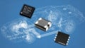
STMicroelectronics has announced their TS33 series, which is a new family of micropower high-precision voltage reference ICs. These voltage reference ICs—which, like other voltage references, are essentially highly accurate LDOs—are described as “micropower” ICs.
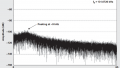
And the current consumption is indeed very low, even at extreme temperatures: 3.9µA (typical) at 25°C, 7.5µA (maximum) from -40°C to +85°C, and 10µA (maximum) from -40°C to +125°C (see the figure below).

Figure 1. Current-consumption specs, from the datasheet (PDF).
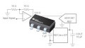
A 3-Pin Device in an 8-Pin Package
Although this voltage reference comes in a QFN8 1.5 × 1.5mm package, which is actually quite small, it's a little puzzling that STMicroelectronics didn't attempt to further trim down the size of the package by reducing the number of unused pins—only three of the eight pins are used! However, I assume that the "unused pins" are only unused by the customer; surely at least some of these pins are utilized for testing and troubleshooting, or other production-related activities, within the walls of ST.

Figure 2. TS33 package and pinout, from the datasheet (PDF).
A Range of Fixed Output Voltages...Coming Soon
While ST's website states that this TS33 family of voltage reference ICs is available in a variety of fixed output voltages (see image below), the datasheet provides ordering information only for two voltage variants, namely, 1.25V and 3.0V (see image below). Furthermore, take note that, according to the datasheet, the 1.25V version is available only upon request.

Figure 3. ST’s website lists a variety of output voltage options.

Figure 4. The TS33 datasheet lists ordering information for only two output voltage variants.
I suspect that ST has valid reasons for initially offering only these two voltage flavors. Perhaps the 1.25V and 3.0V versions are the most popular, and, therefore, ST decided to fine-tune these ICs and gather ample characterization data prior to shifting their focus to the less popular output voltages.
Regardless, contacting ST would be the best approach for getting the most up-to-date information on which parts are currently available.
Output Voltage vs. Input Voltage
As mentioned before, this voltage reference IC is basically an LDO, and one that has 1) a very low dropout voltage (from 50 to 100 mV, depending on operating conditions) and 2) a very tight line regulation spec, i.e., 8ppm/V (typical) for temperatures up to +85°C. See the electrical specifications table below.

Figure 5. TS33 VOUT specifications, from the datasheet (PDF).
A Curious Plot
The following two plots give some additional insight into the TS33’s dropout characteristics. It appears to me, however, that the “output voltage vs. input voltage” plot is unclear and possibly erroneous.
-
Within the figure's description, VOUT is stated to be 3.0V, whereas the plot shows VOUT as being a smidgen above the 3.0V horizontal line; perhaps this discrepancy corresponds to the device’s ±0.15% accuracy?
-
There is no offset between the input voltage and the output voltage. At VIN = 1V, VOUT = 1V; at VIN = 2V, VOUT = 2V; at VIN = 3V, VOUT = 3V. What happened to the dropout voltage? How can any voltage regulator operating under real-world conditions have an output voltage that is identical to the input voltage?
-
The plot is in reference to the "typical application circuit," but no such circuit exists in this datasheet.

Figure 6. Dropout behavior, from the datasheet (PDF).

Figure 7. The lowest dropout voltage is achieved by minimizing load current. Plot taken from the datasheet (PDF).
Output Voltage vs. Temperature
This voltage reference IC is described as being "capable of providing stable and precise output voltages with an initial accuracy of 0.15% over an extended temperature range (-40°C to +125°C)." The trouble is, I'm not exactly sure what is meant by the word initial. Are they trying to say that the accuracy will eventually (slowly, quickly, somewhere in between) get worse? Or does the word initial imply that as the operating conditions (VIN, temperature, humidity...) deviate from ideal conditions the device will become less accurate?

Figure 8. The initial accuracy specification is listed at ±0.15%, although the meaning of "initial" is not clear. Tables taken from the datasheet (PDF).
Before we finish up, it’s worthwhile to point out that this reference voltage IC is subject to a trade-off that characterizes low-power devices in general: noise increases as current consumption decreases. The following valuable insight was shared by one of AAC’s forum members:
"Although the TS33’s low power consumption is impressive, ... it comes at a hefty price: like most other micropower devices, ... these parts are very noisy. For example, the 3 volt version has a noise voltage level of 67 μV peak-to-peak which, when compared to the 1.6 μV noise of Analog Devices' ADR4530B, is pretty poor. This may look like no big deal, but consider: 67 μV peak-to-peak on an output of 3.0 volts is 22 parts-per-million peak-to-peak. If this part is used to supply the reference voltage for a 24-bit ΣΔ ADC, it essentially turns that ADC into a 15-1/2 bit converter.
On the other hand, the ADR4530 requires up to 950 μA to operate, so there's the tradeoff.
I'm sure there are plenty of applications for which the TS33 is appropriate; however, serving as a voltage reference for a high-performance ADC is not one of them."
Have you had a chance to use one of ST’s reference voltage ICs from this TS33 family? If so, leave a comment and tell us about your experiences.
Related Content