Facebook
 Google
 GitHub
 Linkedin
Evaluating the Class AB Output Stage for Piezo Driver Design
We examine the basic requirements of piezoelectric amplifiers and how Class AB operation can meet them.
Piezo actuators are omnipresent in positioning systems. These actuators rely on the inverse piezoelectric effect, a physical transducer mechanism where a material exerts force in response to an electrical charge.
Unfortunately, one cannot simply connect a motion controller directly to the piezo actuator. Instead, we use a piezoelectric amplifier. Also known as a piezo driver or piezo amplifier, this is a key part of any piezo system.
A wide variety of high-power piezo amplifiers exist for us to choose from. In this three-part article series, we'll explore the pros and cons of Class AB versus Class D output stages for these amplifiers. As we'll see, there's no one-size-fits-all-solution.
In this article, we'll introduce the requirements of a piezo driver and examine the Class AB output stage. Our discussion will include both the circuit topology and the way it affects the piezo amplifier's design and performance. In the next article, we'll move to discussing the Class D stage. By the end of this series, the reader should understand the major performance trade-offs and key application areas of both output stage types.
Why a Piezo Driver is Necessary
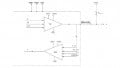
Figure 1 depicts the typical placement of a piezo driver in a precision positioning system.
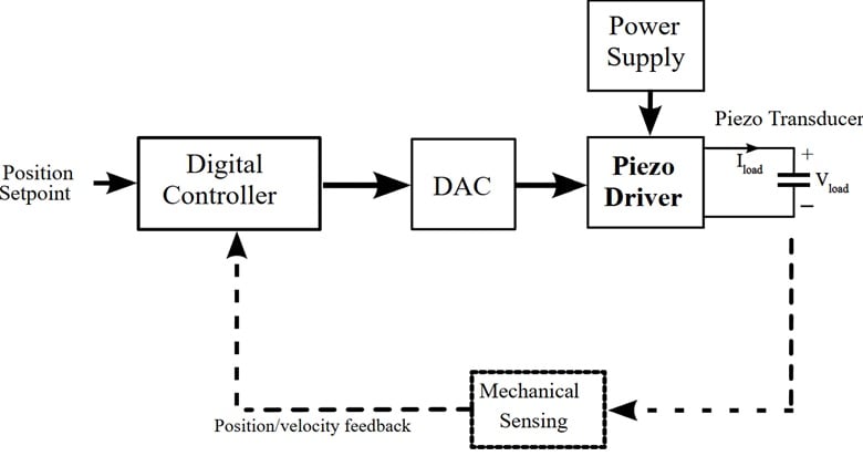
Figure 1. Typical placement of a piezo amplifier in a mechanical positioning system.
The purpose of the driver is to generate an electrical signal for its piezo load. Because there is a close relationship between the applied charge and the mechanical deformation of a piezo device, the most suitable driver is a charge amplifier.
The problem is that piezo devices behave capacitively. This results in a quasi-linear relationship between charge and voltage. In this article, we assume a voltage-to-voltage piezo amplifier with a low-power input voltage (e.g. from a DAC) that is linearly amplified to an output voltage.
The designer should verify whether a voltage amplifier is suitable for the application. Especially in cases without mechanical feedback, the nonlinear Q-V relationship of the piezo load can negatively affect accuracy when a piezo voltage driver is used.
Performance Specifications of a Piezo Amplifier
Before diving into design choices for the driver's output stage, we need a good understanding of the relevant performance aspects.
We've already mentioned that piezo actuators have a capacitive impedance. The size of the driver's load capacitance is largely dependent on the piezo device. Values can range from nanofarads for small piezo actuators to tens of microfarads for large piezo elements. The capacitive load of a piezo amplifier greatly influences several aspects of the design, including required current drive capability, dynamic behavior, frequency stability, and reactive power.
Another important design consideration is the required output voltage range. Piezo actuators typically require a large drive voltage range. Bipolar voltage ranges from –150 V to +150 V are common, as are semi-bipolar ranges from –30 V to +150 V. High-voltage piezos up to kilovolts are emerging as well. This required voltage drive capability impacts the selection of active power devices and the power supply.
The maximum output voltage swing also influences the needed current drive capability of the output stage. The full-power bandwidth (ffpbw) defines the maximum frequency at which the piezo driver can deliver a sinusoidal signal at its full output swing (Vpp,max) without suffering from slew rate limitations. This dynamic nonlinear behavior above ffpbw originates from the finite current (Imax) that can be delivered by the output stage and its power supply. These properties are related through:
$$I_{max}~=~\pi ~\times~f_{fpbw}~\times~C_l~\times~V_{pp,max}$$
Equation 1.
where Cl is the load capacitance.
Not all applications require a driver with high full-power bandwidth. For some applications, it is crucial to precisely control the position of a device while vibration disturbances from the environment interact with the mechanical system. In such cases, there are no large, high-frequency vibrations. Therefore, the full-power bandwidth does not need to be high. Instead, our main concern is the required small-signal bandwidth (Bf) of the piezo driver.
The small-signal bandwidth of the driver's frequency response describes the linearized dynamic behavior. The transfer function of the piezo amplifier output stage will play a role in the bandwidth of the entire amplifier, as it will shape the amplifier's loop gain. See my article "Introduction to SLiCAP for Analog Circuit Design" for a recap of the relationship between the loop gain and the gain of a feedback system.
Unfortunately, every piezo driver will superimpose an unwanted noise component on top of the intended output signal. This is caused by resistive components and active devices, some of which are located in the output stage.
Ripple components are also unwanted spurious signals. Unlike noise, though, ripple is deterministic. We'll consider ripple further later on in this series, when we discuss Class D output stages. Noise and ripple requirements can be critical to high-precision use cases, such as opto-mechanical systems.
Design and Performance of the Class AB Output Stage
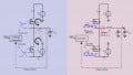
Now that we have some background, let's examine the Class AB driver. The circuit diagram for a Class AB output stage with a capacitive piezo load is shown in Figure 2.
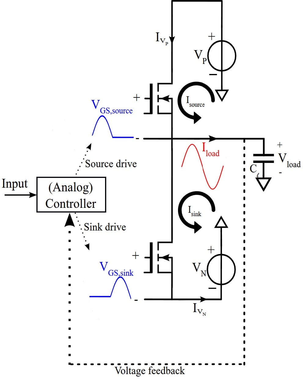
Figure 2. [click to enlarge] Push-pull Class AB output stage used in a voltage feedback amplifier with capacitive piezo load.
This widely used push-pull configuration is similar to the output stage of an op amp. The "push" side, which is the top half, is active when the positive supply (VP) provides a positive current to the load. The "pull" side in the bottom half is active when the load discharges current to the negative supply (VN).
If this were the end of the story, Figure 2 would be a Class B amplifier. In reality, there will be a quiescent current flowing from positive to negative supply, adding a Class A component to the output stage. The circuit is therefore a Class AB configuration.
The configuration in Figure 2 has two NMOS transistors. These MOSFETs operate in the saturation region. The push-stage NMOS has its source connected to the load. Driving the push-stage NMOS with a low-voltage gate-source signal will therefore require an isolated gate driver.
Note that the complete piezo driver typically consists of multiple stages and a voltage feedback loop. Although we are only considering the output stage in this article, all of these stages are important to the bandwidth and distortion performance of the driver.
Power Dissipation and Thermal Management
To understand the operation of the Class AB output stage, let's take a step back and discuss the Class B component. An ideal Class B output stage that is periodically driving a capacitive load (Cl) at peak voltage will consume a total power of:
$$P_{Class~B}~=~C_l~\times~(V_P~+~|V_N|)^2~\times~f_{fpbw}~=~C_l~\times~(V_{pp,max})^2~\times~f_{fpbw}$$
Equation 2.
where:
VP is the positive supply
VN is the negative supply
ffpbw is the full-power bandwidth
Vpp,max is the maximum peak-to-peak signal voltage.
A maximum power efficiency of 78% for Class B operation is often cited in literature. While this is true for resistive loads at peak voltage, it doesn't at all apply to reactive (piezo) loads. After all, the ideal piezo load is a lossless, reactive element. Under periodic excitation, the load capacitance does not consume net power.
Even an ideal Class B amplifier has a power efficiency of zero when its load is purely reactive. The energy returning from the load gets dissipated as heat in the transistors of the Class B output stage.
This is caused by the "push" stage only being able to source current and the "pull" stage only sinking current, in both cases resulting in the power supplies never absorbing power. In other words, the active stage will have a transistor with both drain-source current (IDS) and drain-source voltage (VDS) being non-zero when the load draws current.
Whether this wasted power turning into heat is a problem depends on the application. Some piezo applications require very small, precise movements around an operating point that changes only slowly. Dynamic operation of a Class B push-pull stage at peak-to-peak voltage Vpp and frequency f results in a smaller power consumption:
$$P_{Class~B,~small~excursion}~=~C_l~\times~(V_P~+~|V_N|)~\times~V_{pp}~\times~f$$
Equation 3.
For large-stroke (high Vpp) at fast rate (high f) applications, the power consumption can lead to meaningful design challenges. Even if electrical power is not a scarce resource, the dissipated heat can create thermal management issues. As an example, full excursion of a piezo load Cl = 4 μF between the positive supply VP = 150 V and the negative supply VN = –150 V at a full-power bandwidth ffpbw = 1 kHz results in a power of 360 W!
Even if bulky heat sinks or convective cooling are feasible, the thermal resistance between the junction and the case of the transistors needs to be carefully considered. It may require multiple (stacked) transistors. Thermal connection of the PCB to the heat sink is also an essential consideration.
So far, we have only considered Class B operation. In reality, there will be an overlap between the source and sink phase. This overlap requires a signal-independent quiescent current (IQ) flowing between the positive and negative power supplies. This Class A component improves the amplifier's crossover distortion behavior, at the cost of increased power consumption:
$$P_{quiescent}~=~(V_P~+~|V_N|)~\times~I_Q$$
Equation 4.
If there are constraints on size or mass, a Class AB (or Class B) amplifier might not be a viable choice.
Power Supply Requirements
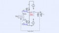
Now that we've discussed power dissipation, let's talk about the power supply. The Class AB stage is compatible with standard power supplies, which should be considered an advantage. To help us understand why, Figure 3 shows the four potential operating modes of power supplies.
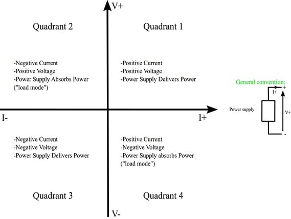
Figure 3. The operating modes of power supplies.
In Quadrants 2 and 4, power is absorbed. Not all power supplies are capable of this. Fortunately, the Class AB output stage for piezo loads does not impose special requirements on its power supply, save for the following:
- The supply must be able to deliver more current than the maximum required load current.
- The supply's DC voltage levels must be compatible with the required voltage swing.
Going back to Figure 2, a load source current (Iload > 0) is always delivered by the positive supply (Quadrant 1 operation). A load sink current (Iload < 0) is delivered by the negative supply (Quadrant 3 operation). In other words, because energy returning from the reactive load is dissipated in the output stage's transistors, power supplies never have to absorb power or act as a load (Quadrant 2 / Quadrant 4 operation).
Wrapping Up
Piezoelectric actuators have become increasingly popular in precision position systems throughout the past years. These transducers convert electrical energy into mechanical motion. To drive these actuators with adequate electrical signals, a piezo amplifier is needed. The application and performance of the positioning system dictate the topology and sizing of the piezo amplifier circuit.
This article, the first of three, highlighted the Class AB piezo driver output stage. While the Class AB stage excels in linearity and absence of switching ripple, it is not suited for large-stroke applications with bulky piezo devices at high full-power bandwidth. Although piezo actuators behave capacitively, periodic charging and discharging can cause thermal management issues in a Class AB stage.
For small-stroke applications requiring precise control around a slowly moving operating point, however, the Class AB output stage can be a good choice. This type of output stage is often encountered in voltage feedback configurations, where it is used to accurately shape the frequency-dependent gain function.
In the next article, we'll consider the use of the switching Class D output stage to drive high-power piezo actuators. The third article in this series will compare the Class AB and Class D output stages for piezo applications.
All images used courtesy of Gilles Ackaert