Facebook
 Google
 GitHub
 Linkedin
Class AB vs. Class D: Understanding the Trade-Offs for Piezo Driver Design
In this article, we explore when to choose a Class AB or Class D output stage for your piezo amplifier design. We'll also examine the Class D stage's power supply requirements.
The type of output stage used in a piezo driver greatly impacts the performance of the piezo positioning system as a whole. When designing a piezo amplifier, it is therefore essential to make a choice that suits the piezo application.
The purpose of this three-part series is to help the designer make an informed decision in this regard. To keep things tightly focused, we have limited ourselves to two options: a Class AB output stage or a Class D one. Both are commonly used in piezo systems.
The first article in this series presented the overall requirements of a piezo driver and examined the operation of the Class AB output stage. In the second article, we discussed the Class D piezo driver. Now, in the third and final article, we'll conclude that discussion by going over the Class D stage's power supply requirements. We'll then compare the strengths and weaknesses of the Class AB and Class D stages for different applications.
Circuit Topology Review
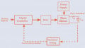
To help refresh our memories, the circuit schematics from the first and second articles are reproduced below. Figure 1 shows the Class AB piezo driver output stage.
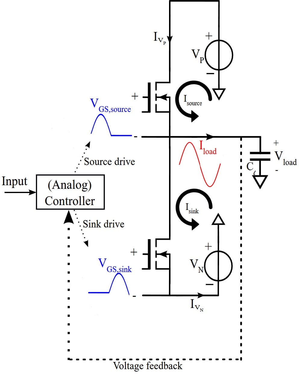
Figure 1. [click to enlarge] Push-pull Class AB output stage, used in a voltage feedback amplifier with capacitive piezo load.
Figure 2 shows the Class D topology introduced in the second article.

Figure 2. [click to enlarge] Class D half-bridge switching output stage, used in a voltage feedback amplifier with capacitive piezo load.
Due to space constraints, our previous discussion of the Class D output stage didn't include its power supply requirements. Before we compare the pros and cons of the two output stage types, let's rectify this.
Power Supply Requirements of the Class D Output Stage
The popularity of the Class D output stage mostly stems from its power efficiency. However, the source of this efficiency also causes a peculiar difficulty in systems with reactive loads. This problem comes down to the need for one or more power supplies that can both deliver and absorb power.
This fundamental need is often overlooked and is best explained with an example. Imagine a positive load current (Iload) and inductor current (ILf). While the high-side circuit is conducting, the current through the positive power supply (IVP) is positive. This requires VP to deliver power.
When the output stage switches to the low-side circuit conducting current, the inductor current stays roughly the same. The inductor current is still positive, but now flows through the negative supply. Therefore, IVN is negative. Current is now flowing from the positive to the negative terminal of the negative supply (VN). The negative supply needs to absorb power rather than provide it.
This power absorption requirement can be partly circumvented by means of a full-bridge configuration with a single positive power supply. Throughout one PWM period, power is then delivered and absorbed by the same power supply terminal and can be smoothed with decoupling capacitors. For resistive loads, which only have net power dissipation, this works without further issues, and no bidirectional power supply is needed.
For capacitive loads, the story unfortunately does not end with this simple countermeasure. Referring back to Figure 2, imagine a positive load voltage (Vload) and a negative load current (Iload), or a negative Vload and positive Iload. In both cases, energy gets returned from the load to one of the power supplies through a negative IVP or negative IVN.
When periodically charging and discharging the capacitive load (for example, at the full-power bandwidth), this will happen half of the time. This is inherently linked to the impedance of the ideal capacitive piezo load:
$$Z_l=~\frac{1}{j2 \pi f C_l}$$
Equation 1.
This impedance has no real part, only an imaginary one.
Voltage and current have a 90 degree quadrature relationship in the ideal piezo load, causing only reactive power:
$$Q~=~\frac{1}{2}Imag(V_{load}I_{load})$$
Equation 2.
and no real power dissipation.
To recover the energy, the amplifier's power supplies need to allow for bidirectional current flow. A full-bridge configuration can eliminate the need for a negative supply. However, in the case of a capacitive piezo load, it will not eliminate the need for the remaining positive power supply to be bidirectional.
This introduces an important power supply requirement when selecting a Class D output stage: the same power supply needs to be able to source and sink current. Multiple options exist, such as regenerative power supplies or local energy storage. Battery systems can be viable as well, depending on the application.
Figure 3 provides an overview of the power supply operating modes with quadrant conventions.
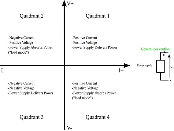
Figure 3. Operating modes of power supplies. In Q2 and Q4, power is absorbed. Not all power supplies have this ability.
In short, a Class D output stage in half-bridge configuration requires two power supplies to cover all four operational quadrants in Figure 3. For a full-bridge configuration, a positive power supply operating in Quadrant 1 (power delivery) and Quadrant 2 (power absorption) suffices.
Output Stage Selection: Trade-Off Overview
With that, we're ready to compare the Class AB and Class D output stages. We'll look at the following design requirements:
- Full-stroke dynamic usage.
- High-frequency ripple.
- Power supply design.
- Electromagnetic interference (EMI).
Once this comparison is complete, we'll wrap up the article with a description of the recommended applications for each output stage.
Full-Stroke/Large-Signal Dynamic Usage
In a Class AB amplifier, the full-stroke reactive power of the capacitive piezo dissipates as heat in the output transistors. The maximum power consumed is given by:
$$P_{max}~=~C_lV^2_{pp} f_{fpbw}$$
Equation 3.
High-power piezo amplifiers are needed when full excursion is part of the application use case, especially for large piezo loads (high Cl), fast dynamic excursion (high ffpbw), and large voltage swing (high Vpp). A Class AB output stage is not suitable for such amplifiers. Its thermal management challenges will result in low reliability, large/bulky heat sinks, or unsafe devices.
In a Class D stage, on the other hand, periodic excitation of the capacitive piezo load results in a periodic exchange of energy between load and power supply. This keeps power dissipation low, even during continuous, long-travel usage. The Class D output stage is very well suited to accommodate large reactive power without excessive heating, allowing compact designs.
Advantage: Class D, very strongly.
High-Frequency Ripple
Class D amplifiers suffer from residual ripple at the PWM frequency, with peak-to-peak values determined by the LC output filter, supply voltage, and PWM frequency. This type of output stage is not ideal for applications that are sensitive to spurious vibrations.
In a Class AB stage, there is no high-frequency switching and therefore no residual ripple. Class AB stages are particularly worth keeping in mind for precision applications that can't tolerate high-frequency disturbances.
However, it's worth noting that precision applications also require high small signal bandwidth and low noise. These performance aspects depend on the design of the full amplifier, not just the output stage. Apart from ripple, Class AB and Class D output stages are both suitable for low noise and high small-signal bandwidth.
Advantage: Class AB.
Power Supply Requirements
Class AB stages are compatible with standard power supplies, which can deliver power but not absorb it. This is an advantage over the Class D stage, which requires a bidirectional supply. In fact, as we discussed earlier in this article, a half-bridge Class D configuration will need more than one power supply.
Advantage: Class AB.
EMI Mitigation
In a Class D output stage, the PWM switching frequency and its harmonics necessitate EMI measures. Class AB stages don't have this problem.
Advantage: Class AB.
Applications
Class AB output stages are commonly used for high-precision mechatronics applications with short stroke movement. They are ideal for dynamic systems requiring high small-signal bandwidth, such as mechanical disturbance (jitter) rejection. With a Class AB output stage, multi-kHz small-signal-bandwidth systems are achievable.
Class AB stages are also suitable for clamping applications. Due to the absence of high-frequency ripple, they avoid dynamic friction coefficients.
If the application calls for large-stroke or long-travel mechanical motion, a Class D output stage is preferable. This is especially the case for heavy piezo loads (high peak current and high peak voltage). Even if electrical power is abundant, heat can cause issues in Class AB designs.
Remember that the importance of each criterion we examined above depends on the application, as well as on the design of the piezo actuation system as a whole.
This article is the final installment of a series on piezo driver output stage selection. All articles in this series are listed below.
- Evaluating the Class AB Output Stage for Piezo Driver Design
- Design and Performance of the Class D Output Stage for Piezo Drivers
- Class AB vs. Class D: Understanding the Trade-Offs for Piezo Driver Design
All images used courtesy of Gilles Ackaert